Chapter: Microprocessor and Microcontroller : I/O Interfacing
D/A and A/D Interface
D/A And A/D Interface:
The
function of an A/D converter is to produce a digital word which represents the
magnitude of some analog voltage or current.
The
specifications for an A/D converter are very similar to those for D/A
converter:
·
The resolution of an A/D converter refers to the
number of bits in the output binary word. An 8-bit converter for example has a
resolution of 1 part in 256.
·
Accuracy and linearity specifications have the same
meaning for an A/D converter as they do for a D/A converter.
·
Another important specification for an ADC is its
conversion time. - the time it takes the converter to produce a valid output
binary code for an applied input voltage. When we refer to a converter as high
speed, it has a short conversion time.
The
analog to digital converter is treated as an input device by the microprocessor
that sends an initialising signal to the ADC to start the analog to digital
data conversation process.
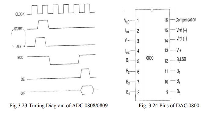
The start
of conversion signal is a pulse of a specific duration. The process of analog
to digital conversion is a slow process, and the microprocessor has to wait for
the digital data till the conversion is over.
After the
conversion is over, the ADC sends end of conversion (EOC) signal to inform the
microprocessor that the conversion is over and the result is ready at the
output buffer of the ADC.
These
tasks of issuing an SOC pulse to ADC, reading EOC signal from the ADC and
reading the digital output of the ADC are carried out by the CPU using 8255 I/O
ports. The time taken by the ADC from the active edge of SOC pulse (the edge at
which the conversion process actually starts) till the active edge of
EOC
signal is called as the conversion delay of the ADC- the time taken by the
converter to calculate the equivalent digital data output from the instant of
the start of conversion is called conversion delay. It may range anywhere from
a few microseconds in case of fast ADCs to even a few hundred milliseconds in
case of slow ADCs.
A number
of ADCs are available in the market, the selection of ADC for a particular
application is done, keeping in mind the required speed, resolution range of
operation, power supply requirements, sample and hold device requirements and
the cost factors are considered.
The
available ADCs in the market use different conversion techniques for the
conversion of analog signals to digital signals.
Parallel converter or flash converter, Successive
approximation and
dual slope
integration
A general
algorithm for ADC interfacing contains the following steps.
1. Ensure
the stability of analog input, applied to the ADC.
2. Issue
start of conversion (SOC) pulse to ADC.
3. Read end
of conversion (EOC) signal to mark the end of conversion process.
4. Read
digital data output of the ADC as equivalent digital output.
It may be
noted that analog input voltage must be constant at the input of the ADC right
from the start of conversion till the end of conversion to get correct results.
This may be ensured by a sample and hold
circuit which samples the analog signal and holds it constant for a
specified time duration. The microprocessor may issue a hold signal to the
sample and Hold circuit. If the
applied
input changes before the complete conversion process is over, the digital
equivalent of the analog input calculated by the ADC may not be correct. If the
applied input changes before the complete conversion process is over, the
digital equivalent of the analog input calculated by the ADC may not be
correct.
·
ADC
0808/0809
The analog to digital converter chips 0808 and 0809 are 8-bit CMOS, successive approximation converters. Successive approximation technique is one of the fast techniques for analog to digital conversion. The conversion delay is 100 μs at a clock frequency of 640
kHz,
which is quite low as compared to other converters.
These
converters do not need any external zero or full scale adjustments as they are
already taken care of by internal circuits. These converters internally have a
3:8 analog multiplexer so that at a time eight different analog inputs can be
connected to the chips. Out of these eight inputs only one can be selected for
conversion by using address lines ADD A, ADD B and ADD C, as shown. Using these
address inputs, multichannel data acquisition systems can be designed using a
single ADC.
The CPU
may drive these lines using output port lines in case of multichannel
applications. In case of single input applications, these may be hard wired to
select the proper input.
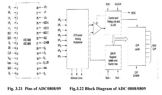
only
positive analog input voltages to their digital equivalents. These chips do not
contain any internal sample and hold circuit. If one needs a sample and hold
circuit for the conversion of fast, signals into equivalent digital quantities,
it has to be externally connected at each of the analog inputs.
INTERFACING DIGITAL TO ANALOG ONVERTERS:
The
digital to analog converters convert binary numbers into their analog
equivalent voltages or currents. Several techniques are employed for digital to
analog conversion.
i. Weighted
resistor network
ii. R-2R
ladder network
iii. Current
output D/A converter
ü Applications
in areas like
· digitally
controlled gains, motor speed control, programmable gain amplifiers, digital
voltmeters, panel meters, etc.
· In a
compact disk audio player for example a 14-or16-bit D/A converter is used to
convert the binary data read off the disk by a laser to an analog audio signal.
· Most
speech synthesizer integrated circuits contain a D/A converter to convert stored
binary data words into analog audio signals.
ü Characteristics:
1. Resolution:
It is a change in analog output for one LSB change in digital input.
It is
given by(1/2n )*Vref.
If n=8 (i.e.8-bit DAC) 1/256*5V=39.06mV
2.
Settling time: It is the time required for the DAC to settle for a full scale
code
change.
DAC 0800
8-bit Digital to Analog converter Features:
i. DAC0800
is a monolithic 8-bit DAC manufactured by National semiconductor.
ii. It has
settling time around 100ms
iii. It can
operate on a range of power supply voltage i.e. from 4.5V to +18V. Usually the
supply V+ is 5V or +12V. The V- pin can be kept at a minimum of - 12V.
iv.Resolution
of the DAC is 39.06mV
Related Topics