Chapter: Microprocessor and Microcontroller : I/O Interfacing
Serial Communication interface: Using 8251
Serial Communication: Using 8251
8251 is a Universal Synchronous and Asynchronous Receiver and Transmitter compatible with Intel’s processors. This chip converts the parallel data into a serial stream of bits suitable for serial transmission. It is also able to receive a serial stream of bits and convert it into parallel data bytes to be read by a microprocessor.
1 Basic Modes of data transmission
a) Simplex
b) Duplex
c) Half
Duplex
a) Simplex mode
Data is
transmitted only in one direction over a single communication channel. For
example, the processor may transmit data for a CRT display unit in this mode.
b) Duplex Mode
In duplex
mode, data may be transferred between two transreceivers in both directions
simultaneously.
c) Half Duplex mode
In this
mode, data transmission may take place in either direction, but at a time data
may be transmitted only in one direction. A computer may communicate with a
terminal in this mode. It is not possible to transmit data from the computer to
the terminal and terminal to computer simultaneously.
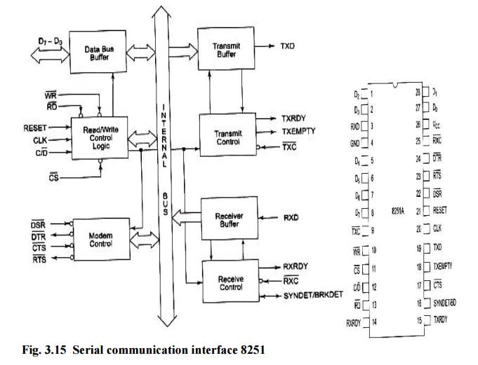
The data
buffer interfaces the internal bus of the circuit with the system bus. The read
/ write control logic controls the operation of the peripheral depending upon
the operations initiated by the CPU decides whether the address on internal
data bus is control address / data address. The modem control unit handles the
modem handshake signals to coordinate the communication between modem and
USART.
The
transmit control unit transmits the data byte received by the data buffer from
the CPU for serial communication. The transmission rate is controlled by the
input frequency. Transmit control unit also derives two transmitter status
signals namely TXRDY and TXEMPTY which may be used by the CPU for handshaking.
The
transmit buffer is a parallel to serial converter that receives a parallel byte
for conversion into a serial signal for further transmission. The receive
control unit decides the receiver frequency as controlled by the RXC input
frequency. The receive control unit generates a receiver ready (RXRDY) signal
that may be used by the CPU for handshaking. This unit also detects a break in
the data string while the 8251 is in asynchronous mode. In synchronous mode,
the 8251 detects SYNC characters using SYNDET/BD pin.
2 Signal Description of 8251
D0 – D7: This is an 8-bit data bus used to
read or write status, command word or data from or to the 8251A.
C / D: (Control Word/Data): This input
pin, together with RD and WR inputs, informs the 8251A that the word on the data bus is either a data or control
word/status information. If this pin is 1, control / status is on the bus,
otherwise data is on the bus.
RD: This active-low input to 8251A is
used to inform it that the CPU is reading either data or status information from its internal registers. This active-low
input to 8251A is used to inform it that the CPU is writing data or control
word to 8251A.
WR: This is an active-low chip select
input of 825lA. If it is high, no read or write operation can be carried out on 8251. The data bus is tristated if
this pin is high.
CLK: This
input is used to generate internal device timings and is normally connected to clock generator output. This input
frequency should be at least 30 times greater than the receiver or transmitter
data bit transfer rate.
RESET: A high on
this input forces the 8251A into an idle state. The device will remain idle till this input signal again goes
low and a new set of control word is written into it. The minimum required
reset pulse width is 6 clock states, for the proper reset operation.
TXC (Transmitter Clock Input): This
transmitter clock input controls the rate at which the character is to be transmitted. The serial data is shifted out on
the successive negative edge of the TXC.
TXD (Transmitted Data Output): This
output pin carries serial stream of the transmitted data bits along with other information like start bit, stop bits
and parity bit, etc.
RXC (Receiver Clock Input): This receiver
clock input pin controls the rate at which the character is to be received.
RXD (Receive Data Input): This
input pin of 8251A receives a composite stream of the data to be received by 8251 A.
RXRDY (Receiver Ready Output): This
output indicates that the 8251A contains a
character to be read by the CPU.
TXRDY - Transmitter Ready: This output signal indicates to the CPU that the internal circuit of the transmitter is ready to accept a new character for transmission from the CPU.
DSR - Data
Set Ready: This is normally used to check if data set is ready when communicating with a modem.
DTR - Data Terminal Ready: This is
used to indicate that the device is ready to accept data when the 8251 is communicating with a modem.
RTS - Request to Send Data: This
signal is used to communicate with a modem.
TXE- Transmitter Empty: The TXE
signal can be used to indicate the end of a
transmission mode.
3 Operating Modes of 8251
1. Asynchronous
mode
2. Synchronous
mode
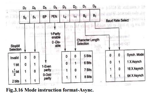
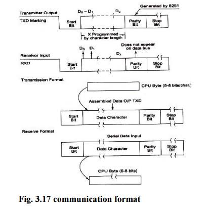
Asynchronous Mode (Transmission)
When a
data character is sent to 8251A by the CPU, it adds start bits prior to the
serial data bits, followed by optional parity bit and stop bits using the
asynchronous mode instruction control word format. This sequence is then
transmitted using TXD output pin on the falling edge of TXC.
Asynchronous Mode (Receive)
A falling edge on RXD input line marks a start bit.
The receiver requires only one stop bit to mark end of the data bit string,
regardless of the stop bit programmed at the transmitting end. The 8-bit
character is then loaded into the into parallel I/O buffer of 8251.
RXRDY pin
is raised high to indicate to the CPU that a character is ready for it. If the
previous character has not been read by the CPU, the new character replaces it,
and the overrun flag is set indicating that the previous character is lost.
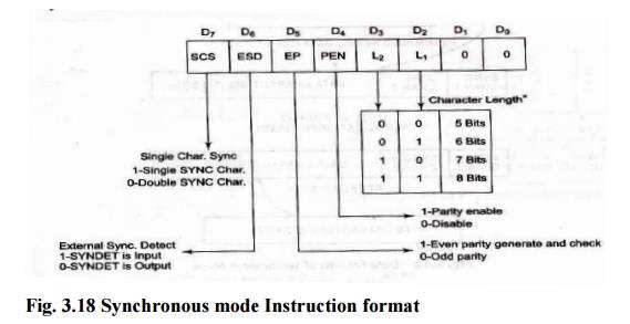
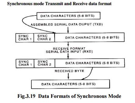
Synchronous Mode (Transmission)
The TXD
output is high until the CPU sends a character to 8251 which usually is a SYNC
character. When CTS line goes low, the first character is serially transmitted
out. Characters are shifted out on the falling edge of TXC .Data is shifted out
at the same rate as TXC , over TXD
output line. If the CPU buffer becomes empty, the SYNC character or characters
are inserted in the data stream over TXD output.
Synchronous Mode (Receiver)
In this
mode, the character synchronization can be achieved internally or externally.
The data on RXD pin is sampled on rising edge of the RXC. The content of the
receiver buffer is compared with the first SYNC character at every edge until
it matches. If 8251 is programmed for two SYNC characters, the subsequent
received character is also checked. When the characters match, the hunting
stops. The SYNDET pin set high and is reset automatically by a status read
operation. In the external SYNC mode, the synchronization is achieved by
applying a high level on the SYNDET input pin that forces 8251 out of HUNT
mode. The high level can be removed after one RXC cycle. The parity and overrun
error both are checked in the same way as in asynchronous mode.
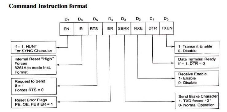
Command Instruction Definition
The
command instruction controls the actual operations of the selected format like
enable transmit/receive, error reset and modem control. A reset operation
returns 8251 back to mode instruction format.
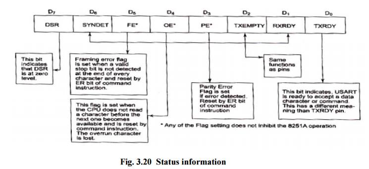
Status Read Definition
This
definition is used by the CPU to read the status of the active 8251 to confirm
if any error condition or other conditions like the requirement of processor
service has been detected during the operation.
Related Topics