Chapter: VLSI Design : CMOS Testing
Important Short Questions and Answers: VLSI Design - CMOS Testing
1. Give the basic nMOS PLA structure.

The basic
PLA structure consists of an AND plane driving an OR plane. The terminology
corresponds to a sum of products (SOP) realization of the desired function. The
SOP realization converts directly into a NAND-NAND implementation. When a
product of sums (POS) realization is desired, it can be implemented in OR-AND
or NOR-NOR logic. In either case, the first array is referred to as the AND
plane, and the second array as the OR plane. The line connecting the AND plane
to the OR plane are called the product lines.
2. What do you mean by CMOS PLA.
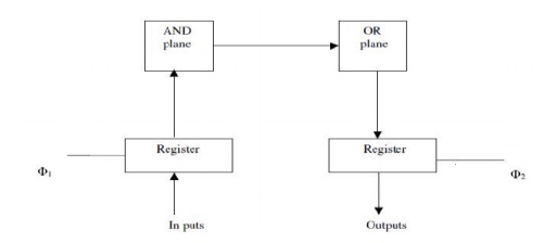
The basic
CMOS PLA is obtained by providing a well and replacing the pull-up devices in
the NAND-NAND array or in the NOR- NOR array with enhancement mode pMOS
devices. The CMOS array can be precharged or not, and can be clocked 2 AND
plane OR plane Register Register In puts Outputs 1 with the same two-phase
clocking scheme as used for the MOS PLA. CMOS PLA design offers many more
varieties of layout than does nMOS.
3. Define finite state machine.
When
feedback is added to the AND OR PLA structure, the PLA becomes a finite state
machine (FSM). An FSM can be designed as a Mealy Machine or a Moore Machine.
The Mealy machine has outputs, which may change with input changes in an
asynchronous manner and cause erroneous behavior. Hence, the Mealy machine
should be avoided whenever possible. The Moore machine has outputs which depend
upon and change only with state changes, since all the outputs of the
Boolean-logic block go through a state register, and are synchronously clocked.
4. What are the importance of the PLA/FSM in VLSI?
(i) Regularity
: It has a standard, easily expandable layout.
(ii) Convenience
: Little design effort is required.
(iii) Compacted
: It is efficient for small circuits.
(iv) Modularity
: It makes it possible to design hierarchical PLAs and FSMs into large
sequential systems.
(v) Suitability
to being computer generated.
5. Give
the structure of a CPLD.
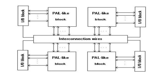
A CPLD comprises multiple circuit
blocks on a single chip, with internal wiring resources to connect the circuit
blocks. Each circuit block is similar to a PLA or a PAL.It includes four PAL like
blocks that are connected to a set of interconnection wires. Each PAL like
block is also connected to a sub circuit labeled I/O block, which is attached
to a number of the chip’s input and output pins

6. Give the CPLD packages available.
a. PLCC package: The PLCC package has pins that “wrap around” the
edges of the chipon all four of its sides. The socket that houses the PLCC is
attached by solder to the circuit board, and the PLCC is held in the socket by
friction.
b. quad flat pack package: The QFP
package has pins on all four sides, and they extendoutward from the package,
with a downward-wiring
shape.
The QFP’s pins are much thinner than those on a PLCC, which means that the
package can support a larger number of pins; QFPs are available with more than
200 pins.
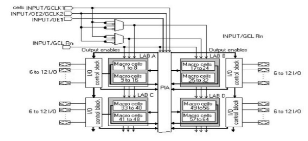
7. Give the structure of MAX 7000 CPLD.

8. What is meant by FPGA?
A field
programmable gate array (FPGA) is a programmable logic device that supports
implementation of relatively large logic circuits. FPGAs can be used to
implement a logic circuit with more than 20,000 gates whereas a CPLD can
implement circuits of upto about 20,000 equivalent gates. FPGAs are quite
different from CPLDs because FPGAs do not contain AND or OR planes. Instead,
they provide logic blocks for implementation of the required functions.
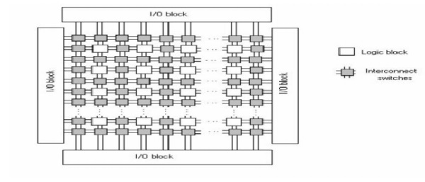
9. Give the general structure of FPGA.

10.
What are the different commercial
FPGA products?
Manufacturer
FPGA products www Locator
Actel
Act 1,2 and 3,MX,SX www.actel.com
Altera
FLEX6000,8000 and 10k APEX 20kwww.altera.com
Atmel
AT6000, AT40k www.ateml.com
Lucent
ORCA 1,2 and 3 www.lucent.com
QuickLogic
pASIC 1,2 and 3 www.quicklogic.com
Vantis
VFI www.vantis.com
Xilinx
XC3000,XC4000,XC5200,Virtexwww.xilinx.com
11.
What are
the types of reprogrammable GA?
Ad-hoc
Array and Structured Array are the two types of Reprogrammable Gate Array.
12.
What is
the type’s o FPLA?
I.PROM
[Programmed Read-Only Memory]
PAL
[Programmed Array Logic]
13.
What are
the applications of PAL?
i.
Control logic application
ii.
Input/Output
iii. Data-path
logic
15. What is finite state machine (FSM)?
When
feedback is added to AND-OR PLA structure, then it becomes FSM.
16.
What are
the characteristics of PLA/FSM?
i.
Regularity
ii.
Modularity
iii. Suitability
iv. Efficiency
17.
What is
CLB?
CLB means
Configurable Logic Block.
18. Define mealy machine?
In mealy
machine, output may change with the change in the input asynchronously.
19. Define moore machine?
In moore
machine, output can be changed when state is changed.
20. What is HDL?
VHSIC
Hardware description Language.
21. What is VHSIC?
Very High
Sped Integrated Circuits.
22.
What are
the various operators in VHDL?
i.
Logical operators
ii.
Relational operators
iii. Shift
operators
iv. Adding
operators
v.
Multiplying operators
23.
What are
the data types available in VHDL?
i.
Scalar type
ii.
Composite type
iii. Access
type
iv. File type
24.
What are
the types of subprograms?
Functions
and Procedures are types of subprograms.
25. What is the use of actual?
Actual in
a subprogram call is used to pass the values from and to a subprogram.
Related Topics