Chapter: Linear Integrated Ciruits : Characteristics of op-amp
Important Short Questions and Answers: Characteristics of op-amp
Characteristics of Op-Amp
1.What are the advantages of ICs over discrete
circuits.?
1.
Minimization & hence increased equipment
density.
2.
Cost reduction due to batch processing.
3.
Increased system reliability
4.
Improved functional performance.
5.
Matched devices.
6.
Increased operating speeds
7.
Reduction in power consumption
2.
What is
OPAMP?
An
operational amplifier is a direct coupled high gain amplifier consisting of one
or more differential amplifiers , followed by a level translator and an output
stage.It is a versatile device that can be used to amplify ac as well as dc
input signals & designed for computing mathamatical functions such as
addition, subtraction , multiplication, integration & differentiation
.
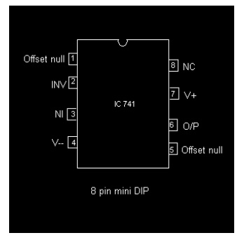
3.Draw the pin configuration of IC741.

4. List out the ideal characteristics of OPAMP?
( i )Open
loop gain infinite
(ii)Input
impedance infinite
(iii)Output
impedance low
(iv)Bandwidth
infinite
(v)Zero offset,ie,
Vo=0 when V1=V2=0
5.what are the different kinds of packages of
IC741? a)Metal
a) can
(TO) package
b) Dual-
in- line package
c)Flat
package or flat pack
6.What are theassumptions made from ideal opamp
characteristics?
i)The
current drawn by either of the input terminals(non-inverting/inverting) is
negligible.
ii)the
potential difference between the inverting & non- inverting input terminals
is zero.
7. Mention some of the linear applications of op –
amps :
Adder,
subtractor, voltage –to- current converter, current –to- voltage converters,
instrumentation amplifier, analog computation ,power amplifier, etc are some of
the linear op-amp circuits.
8.Mention some of the non – linear applications of
op-amps:-
Rectifier,
peak detector, clipper, clamper, sample and hold circuit, log amplifier, anti
–log amplifier, multiplier are some of the non – linear op-amp circuits.
9.What are the areas of application of non- linear
op- amp circuits?
¯
industrial instrumentation
¯
Communication
¯
Signal processing
10.What happens when the common terminal of V+
and V- sources is not grounded?
If the
common point of the two supplies is not grounded, twice the supply voltage will
get applied and it may damage the op-amp.
11.Define input offset voltage.
A small
voltage applied to the input terminals to make the output voltage as zero when
the two input terminals are grounded is called input offset voltage.
12. Define input offset current. State the reasons
for the offset currents at the input of the op-amp.
The
difference between the bias currents at the input terminals of the op-amp is
called as input offset current. The input terminals conduct a small value of dc
current to bias the input transistors.Since the input transistors cannot be
made identical,there exists a difference in bias currents.
13. Define CMRR of an op-amp.
The
relative sensitivity of an op-amp to a difference signal as compared to a common
–mode signal is called the common –mode rejection ratio. It is expressed in
decibels.
CMRR=
Ad/Ac
14.In practical op-amps, what is the effect of high
frequency on its performance?
The open-
loop gain of op-amp decreases at higher frequencies due to the presence of
parasitic capacitance. The closed- loop gain increases at higher frequencies
and leads to instability.
15. What is the need for frequency compensation in
practical op-amps?
Frequency
compensation is needed when large bandwidth and lower closed loop gain is
desired. Compensating networks are used to control the phase shift and hence to
improve the stability.
16.Mention the frequency compensation methods.
*Dominant-pole
compensation
*Pole-
zero compensation.
17.What are the merits and demerits of
Dominant-pole compensation? *noise immunity of the system is
improved.
*Open-loop
bandwidth is reduced.
18.Define slew rate.
The slew
rate is defined as the maximum rate of change of output voltage caused by a
step input voltage.An ideal slew rate is infinite which means that op-amp’s
output voltage should change instantaneously in response to input step voltage.
19.Why IC 741 is not used for high frequency
applications?
IC741 has
a low slew rate because of the predominance of capacitance present in the
circuit at higher frequencies. As frequency increases the output gets distorted
due to limited slew rate.
20.What causes slew rate?
There is
a capacitor with- in or outside of an op-amp to prevent oscillation.It is this
capacitor which prevents the output voltage from responding immediately to a
fast changing input.
21.Define thermal drift.
The bias
current , offset current & offset voltage change with temperature. A
circuit carefully nulled at 25oC may not remain so when the
temperature raises to 35oC.This is called thermal drift . Often,
offset current drift is expressed in nA/ o C and offset voltage
drift in mV/ oC.
22.Define supply voltage rejection ratio(SVRR)
The
change in OPAMP’s input offset voltage due to variations in supply voltage is
called the supply voltage rejection ratio.It is also called Power Supply
Rejection Ratio(PSRR) or Power Supply Sensitivity(PSS).
Related Topics