Chapter: Linear Integrated Ciruits : Characteristics of op-amp
DC Characteristics of op-amp
DC Characteristics of op-amp:
Current
is taken from the source into the op-amp inputs respond differently to current
and voltage due to mismatch in transistor.
DC output
voltages are,
1.
Input bias current
2.
Input offset current
3.
Input offset voltage
4.
Thermal drift
1. Input bias current:
The
op-amp‘s input is differential amplifier, which may be made of BJT or FET.
·
In an ideal op-amp, we assumed that no current is
drawn from the input terminals.
· The base currents entering into the inverting and non-inverting terminals (IB-& IB+ respectively).
· Even though both the transistors are identical, IB- and IB+ are not exactly equal due to internal imbalance between the two inputs.
· Manufacturers specify the input bias current IB
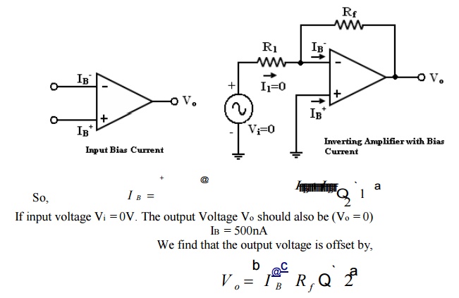
Op-amp with a 1M feedback resistor
V0 = 5000nA X 1M = 500mV
The
output is driven to 500mV with zero input, because of the bias currents.
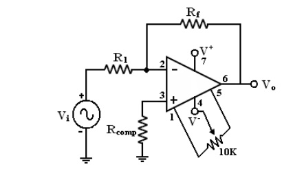
In
application where the signal levels are measured in mV, this is totally
unacceptable. This can be compensated. Where a compensation resistor Rcomp has
been added between the non-inverting input terminal and ground as shown in the
figure below.
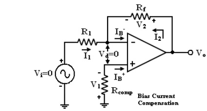
Current IB+ flowing through the compensating resistor Rcomp, then by KVL we
-V1+0+V2-Vo
= 0 (or)
Vo
= V2 – V1 ——>(3)
By
selecting proper value of Rcomp, V2 can be cancelled with
V1 and the Vo = 0. The value of Rcomp is
derived a
V1 =I=+Rcomp (or)
IB+
= V1/Rcomp
——>(4)
The node
=a‘ is at voltage (-V1). Because the voltage at the non-inverting
input terminal is (-V1). So with Vi = 0 we get,
I1
= V1/R1 ——>(5)
I2
= V2/Rf ——>(6)
For
compensation, Vo should equal to zero (Vo = 0, Vi = 0).
i.e. from equation (3) V2 = V1. So that,
I2
= V1/Rf ——>(7)
KCL at
node =a‘ gives,
IB-=
I2 + I1
IB-
= RfR1
Assume IB-
= IB+ and using equation (4) & (8) we get
Rcomp
= R1 + Rf
Rcomp
= R1 || Rf --->(9)
i.e. to
compensate for bias current, the compensating resistor, Rcomp
combination of resistor R1 and Rf.
2. Input offset current:
Bias
current compensation will work if both bias currents IB+ and IB-
are equal.
Since the
input transistor cannot be made identical. There will always be some small
difference between IB+ and IB-.
This difference is called the offset current
|Ios|
= IB+ -IB- -à(10)
Offset
current Ios for BJT op-amp is 200nA and for FET op-amp is 10pA. Even
with bias current compensation, offset current will produce an output voltage
when Vi = 0.
Equation
(16) the offset current can be minimized by keeping feedback resistance small.
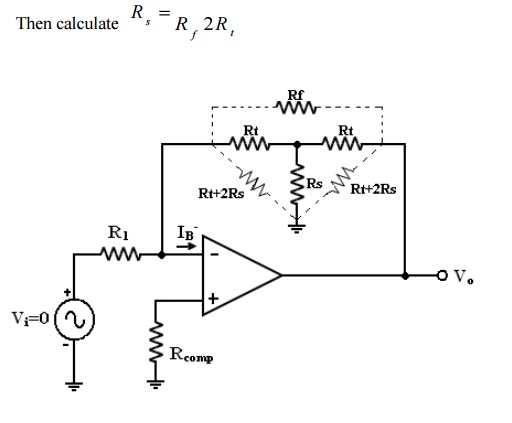
·
Unfortunately to obtain high input impedance,
R1 must be kept large.
·
R1
large, the feedback resistor Rf must also be high. So as to
obtain reasonable gain.
The
T-feedback network is a good solution. This will allow large feedback
resistance, while keeping the resistance to ground low (in dotted line).
·
The T-network provides a feedback signal as if the
network were a single feedback resistor.
By T to Π
conversion,
To design
T- network first pick Rt<<Rf/2
3. Input offset voltage:
Inspite
of the use of the above compensating techniques, it is found that the output
voltage may still not be zero with zero input voltage [Vo ≠ 0 with Vi
= 0]. This is due to unavoidable imbalances inside the op-amp and one may have
to apply a small voltage at the input terminal to make output (Vo) =
0.
This
voltage is called input offset voltage Vos. This is the voltage
required to be applied at the input for making output voltage to zero (Vo
= 0).
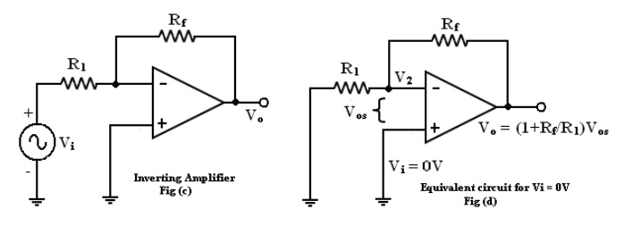
Let us
determine the Vos on the output of inverting and non-inverting amplifier. If Vi
= 0 (Fig (b) and (c)) become the same as in figure (d).
Total output offset voltage:
The total
output offset voltage VOT could be either more or less than the offset voltage
produced at the output due to input bias current (IB) or input
offset voltage alone(Vos).
This is
because IB and Vos could be either positive or negative
with respect to ground. Therefore the maximum offset voltage at the output of
an inverting and non-inverting amplifier (figure b, c) without any compensation
technique used is given by many op-amp provide offset compensation pins to
nullify the offset voltage.
·
10K potentiometer is placed across offset null pins
1&5. The wipes connected to the negative supply at pin 4.
·
The position of the wipes is adjusted to nullify
the offset voltage
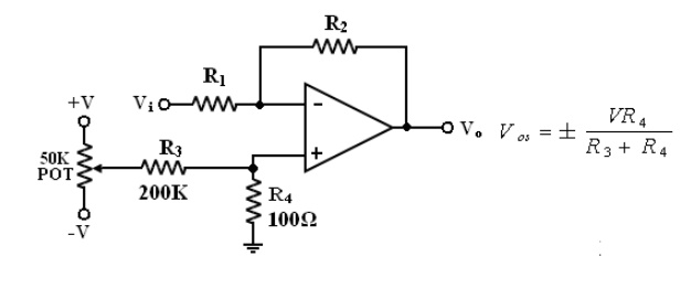
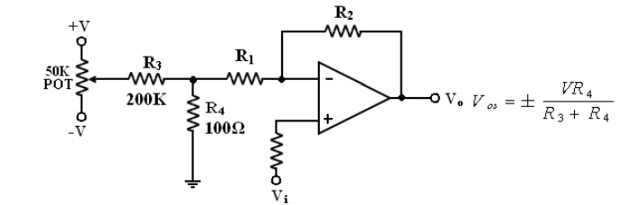
When the
given (below) op-amps
does not have
these offset null
pins, external balancing techniques are used
Balancing circuit:
Inverting amplifier:
Non-inverting amplifier:
4. Thermal drift:
·
Bias current, offset current, and offset voltage
change with temperature.
·
A circuit carefully nulled at 25ºC may not remain.
So when the temperature rises to 35ºC. This is called drift.
·
Offset current drift is expressed in nA/ºC.
·
These indicate the change in offset for each degree
Celsius change in temperature.
Related Topics