Chapter: VLSI Design : Circuit Characterization and Simulation
Device and Circuit Characterization
DEVICE AND CIRCUIT
CHARACTERIZATION
The
modeling procedure is introduced in this chapter, taking into consideration the
requirements for a good MOSFET analog model, discussed in the previous chapter.
We note here two main aspects of our modeling approach;
a. The
model must describe accurately all the operating regions in order to be
integrated in a circuit simulator.
b. The
current, conductance, and transconductance must be continuous in all regions of
operation.
Our main
goal in this chapter is to determine the drain current for any combination of
terminal voltages. The chapter is divided into two main parts.
Throughout
the first part, it is assumed that the channel is sufficiently long and wide,
so that edge effects are confined to a negligible part of it.
While in
the second part we incorporate the short and narrow channel effects to the
model. We also assume that the substrate is uniformly doped.
The
doping concentration will be assumed to be p-type and the modification to non
uniform doping will be discussed later in this chapter.
1. Gradual Channel
approximation (GCA)
Analytical
or semi-analytical modeling of MOSFET characteristics is usually based on the
so-called Gradual Channel Approximation (GCA).
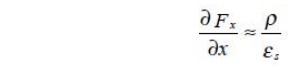
In this
approximation, we assume that the gradient of the electric field in the y
direction, ∂F/∂y is much smaller than the gradient of the electric field in the
x direction,∂F/∂x.
Which
enable us to determine the inversion and depletion charge densities under the
gate in terms of a one-dimensional electrostatic problem for the direction
perpendicular to the channel? By applying of the two dimensional Poisson's
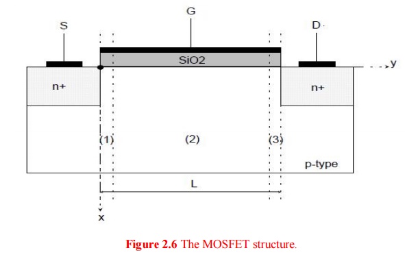
equation for the semiconductor, refer to Fig. 2.1 region (2),
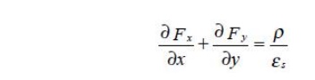
if we
assume that the GCA is valid equation 2.2.1 may be approximated to the
following one dimensional differential equation
we
approach the source and drain junctions, the GCA becomes invalid (Fig. 2.11.1
regions (1) and (3)) because of the increasing longitudinal field due to the pn
junctions which make ∂F/∂y comparable or even larger than ∂F/∂x .
However,
for the long channel MOSFET's these transition regions can be neglected with
respect to the total length of the device. In order to account for the effect
of these regions, it is necessary to use two dimensional analysis requiring a
numerical solution.
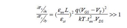
2. Validity of the GCA
The
validity of GCA can be checked by making rough estimates of the variation in
the longitudinal and vertical field components. We will establish expressions
that allow the GCA to be checked under strong inversion.
3. The long channel
current model
The
derivation of the dc drain current relationship recognizes that, in general,
the current in the channel of a MOSFET can be caused by both drift and
diffusion current. In an NMOSFET we may assume the following
resonableapproximation :
i- The
drain current is mainly carried by electrons .
ii- The
current flows almost in the y direction.
iii- No
sources or sinks in the channel.
Note that
in weak inversion the surface potential along the channel in long channel
MOSFETs is almost constant. Thus ∂Fy/∂y is very small, implying that
∂Fy/∂y<<∂Fx/∂x.
T hus in
long channel MOSFET the GCA is valid both in strong and weak inversion regions
. Which enable us to reach to the following general relationship of drain
current.
4. General
Drift-Diffusion current equation in MOSFET:
This is
the drift-diffusion drain current of the form
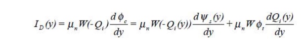
where μn
is the electron surface mobility in the channel, W is the channel width, Qi is
the inversion charge density per unit area, φc is the quasi Fermi potential
(the difference between Efn at the surface of the semiconductor a d Efp in the
bulk of the semiconductor), ψs is the surface potential referenced to the bulk
potential, and φt is the thermal voltage (=kT/q).
The first
term is the drift current component, while the second term is the diffusion
current component. In both components, μn is the electrons' surface mobility
being less than the mobility in the bulk due to surface scattering.
5. Voltage-Charge
equation from the Transverse electric field:
In order
to eliminate the electron charge density Qi term in the current charge
equation, a second relationship is required that relates the electron charge
density to the applied potentials.
Using the
relationship between voltage and charge appearing across the MOS capacitor we
have
Cox (VG
-φ ms -ψ s )= -(Qi+QB+Qox+Qit )
where VG
is the gate voltage referenced to the bulk potential, φms is the metal
semiconductor work function difference, QB is the depletion (bulk impurity)
charge density per unit area, Qox is the sum of the effective net oxide charge
per unit area at the Si-SiO2 interface, and Qit is the interface trapped charge
density per unit area.
Different
approximations have been introduced in order to express the different MOS
charges (QB, Qox, Qit) in terms of the applied voltages, then using eq. to
compute the inversion charge density Qi.
The resulting charge is then used in eq.to determine the drain current; Four main approaches then follow, after them we shall discuss the proposed approach recently developed in ICL1 and modified by this work.
Related Topics