Chapter: VLSI Design : Circuit Characterization and Simulation
Device Models - VLSI Design
DEVICE MODELS
The motivation
for this investigation stems from three main concerns:
1. The
usual parameterization of device models for device and circuit simulation
causes problems due to the interdependence of the parameters.
It is not
physically realistic to change any one parameter without determining the change
in the process technology that would produce such a change in the parameter.
Then all
the other parameters which also depend on this change in the technology must be
adjusted accordingly.
In
addition, it is quite difficult to determine the effect of a specific change in
a new technology since the available parameters each depend on a number of
technology parameters.
2. The
predictive performance of present models is not good. It has usually been
necessary to fabricate devices in any chosen technology, and extract
parameters, and then fit the model to this specific technology by use of
additional “adjustment” parameters.
Of
course, this procedure is reasonable and useful once a technology has been
chosen. However, it would be useful if the model could produce fairly accurate
results if only the process specifications are used.
Without
such predictive accuracy it is difficult to make an initial choice of
technology.
3. Most
models have been developed for digital applications where devices operate above
threshold and therefore are not strongly temperature sensitive.
This
causes problems for modeling analog circuits which use sub threshold operation.
In particular, the temperature dependence of sub threshold behavior has not
been fully explored. In many models some parameters which are temperature
dependent have been assumed to be constant.
Device
and circuit models are all based on the physical properties of semiconductor
materials, the dimensions of the devices, and on theoretical and empirical
equations which are intended to model electrical behavior.
The
distinction between theoretical and empirical equations is often unclear. Most
of the equations are substantially empirical.
Of all
the equations, one of the most fundamental, and problematic, is the equation
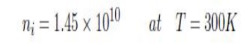
for ni, the intrinsic carrier concentration of asemiconductor.
The
definition of ni derives from the thermodynamic equilibrium of electron and
hole formation, based on the fact that the energy gap is a Gibbs energy. The
equilibrium equation is
np=NcNve-Eg/kt
ni=(np)1/2
where n
is the electron concentration, p is the hole concentration, Nc is the density
of effective states in the conduction band, Nv is the density of effective
states in the valence band, Eg is the band gap, k is Boltzmann’s constant and T
is the absolute temperature.
The
carrier concentration is then given by It would appear to be a simple matter to
substitute Si values for Nc, Nv, Eg, and the value of the constant kT to obtain
an accurate value of ni.
However,
the theoretical and experimental knowledge required for accurate values of Nc
and Nv is even now incomplete. In the early 1960’s, when Si-based circuits were
beginning to be designed and fabricated very little was known about Nc and Nv,
but estimates were required for practical use. This led to approximations based
on work. The key approximation was that chosen by Grove in . This approximation
is the still widely used
1. Determination of
Intrinsic Carrier Concentration (ni)
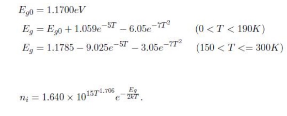
The
empirical expressions for Eg from Bludau and for Nc and Nv from Sproul and
Green provide the values needed for equation (2.1). Our derivation of the
equation for ni follows Green. Therefore, the exciton binding energy term,
using the value Exb = 14.7meV, is included in the band gap, Eg.
In the
past, this term has either been neglected, or in some cases a value of 10meV
has been used. Green [9] and Sproul and Green are by far the best references
for the history, theory, and experimental measurements leading to reliable
values for ni. Thus, the equations are:
Related Topics