Chapter: Linear Integrated Ciruits : Application of Op-Amp
Comparator
Comparator
To
obtain for better
performance, we shall
also look at
integrated designed specifically
as comparators and converters. A comparator as its name implies,
compares a signal voltage on one input of an op-amp with a known voltage called
a reference voltage on the other input.
Comparators
are used in circuits such as,
Digital
Interfacing Schmitt Trigger Discriminato Voltage level detector and oscillators
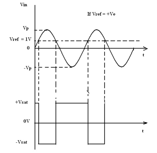
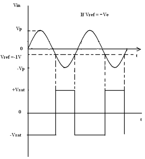
1. Non-inverting Comparator:
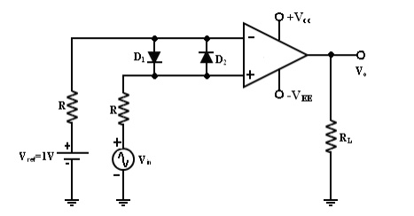
A fixed
reference voltage Vref of 1 V is applied to the negative terminal
and time varying signal voltage Vin is applied tot the positive
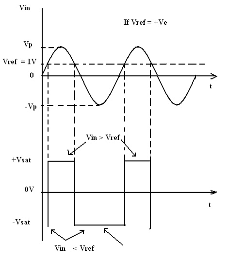
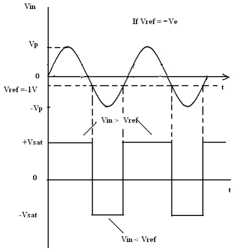
terminal. When Vin is less than Vref the output becomes V0
at –Vsat [Vin < Vref => V0
(-Vsat)]. When Vin is greater than Vref, the
(+) input becomes positive, the V0 goes to +Vsat. [Vin
> Vref=> V0 (+Vsat)]. Thus the V0
changes from one saturation level to another. The diodes D1 and D2
protects the op-amp from damage due to the excessive input voltage Vin. Because
of these diodes, the difference input voltage Vid of the op-amp
diodes are called clamp diodes. The resistance R in series with Vin is used to
limit the current through D1 and D2 . To reduce offset
problems, a resistance Rcomp = R is connected between the (-ve)
input and Vref.
Input and Output Waveforms:
2. Inverting Comparator:
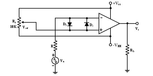
This fig
shows an inverting comparator in which the reference voltage Vref is
applied to the (+) input terminal and Vin is applied to the (-) input terminal.
In this circuit Vref is obtained by using a 10K potentiometer that
forms a voltage divider with dc supply volt +Vcc and -1 and the
wiper connected to the input. As the wiper is moved towards +Vcc,
Vref becomes more positive. Thus a Vref of a desired amplitude and
polarity can be obtained by simply adjusting the 10k potentiometer
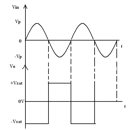
3. Zero Crossing Detector: [ Sine
wave to Square wave converter]
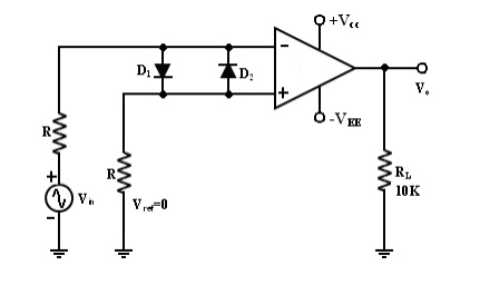
One of
the application of comparator is the zero crossing detector or ―sine wave to
Square wave Converter . The basic comparator can be used as a zero crossing
detector by setting Vref is set to Zero. (Vref =0V).
This Fig
shows when in what direction an input signal Vin crosses zero volts.
(i.e) the o/p V0 is driven into negative saturation when the input
the signal Vin passes through zero in positive direction. Similarly,
when Vin passes through Zero in negative direction the output V0
switches and saturates positively.
Drawbacks of Zero- crossing
detector:
In some
applications, the input Vin may be a slowly changing waveform, (i.e)
a low frequency signal. It will take Vin more time to cross 0V,
therefore V0 may not switch quickly from one saturation voltage to
the other. Because of the noise at the op-amp‘s input terminals the output V0
may fluctuate between 2 saturations voltages +Vsat and –Vsat.
Both of these problems can be cured with the use of regenerative or positive
feedback that cause the output V0 to change faster and eliminate any
false output transitions due to noise signals at the input. Inverting
comparator with positive feedback . This is known as ―Schmitt Trigger .
Schmitt Trigger: [Square Circuit]
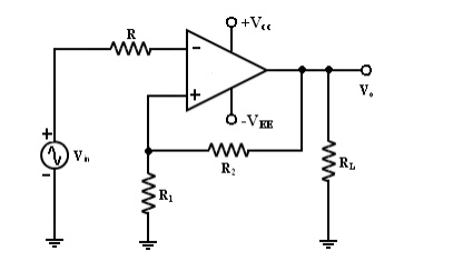
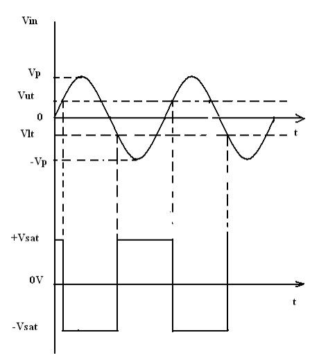
This
circuit converts an irregular shaped waveform to a square wave or pulse. The
circuit is known as Schmitt Trigger or squaring circuit. The input voltage Vin
triggers (changes the state of) the o/p V0 every time it exceeds
certain voltage levels called the upper threshold Vut and lower threshold
voltage. These threshold voltages are obtained by using theh voltage divider R1 – R2, where the voltage across R1 is
feedback to the (+) input.
The
voltage across R1 is variable reference threshold voltage that
depends on the value of the output voltage. When V0 = +Vsat,
the voltage across R1 is called ―upper threshold voltage Vut.
The input voltage Vin must be more positive than Vut in order to
cause the output V0 to switch from +Vsat to –Vsat. As
long as Vin< Vut , V0 is at +Vsat, using
voltage divider rule,
V0
is at –Vsat. Vlt is given by the following eqn.
Thus, if
the threshold voltages Vut and Vlt are made larger than the input noise voltages,
the positive feedback will eliminate the false o/p transitions. Also the
positive feedback, because of its regenerative action, will make V0 switch
faster between +Vsat and –Vsat. Resistance Rcomp
R1
|| R2 is used to minimize the offset problems. The comparator with
positive feedback is said texhibit hysteresis, a dead band condition. (i.e)
when the input of the comparator exceeds Vut its output switches
from +Vsat to –Vsat and reverts to its original state, +Vsat
when the input goes below Vlt. The hysteresis voltage is equal to
the difference between Vut and Vlt.
Related Topics