Physics Practical Experiment - Characteristics of a NPN-Junction Transistor in Common Emitter Configuration | 12th Physics : Practical
Chapter: 12th Physics : Practical
Characteristics of a NPN-Junction Transistor in Common Emitter Configuration
CHARACTERISTICS OF A NPN-JUNCTION
TRANSISTOR IN COMMON EMITTER CONFIGURATION
AIM
To
study the characteristics and to determine the current gain of a NPN junction
transistor in common emitter configuration.
APPARATUS REQUIRED
Transistor
- BC 548/BC107, bread board, micro ammeter, milli ammeter, voltmeters, variable
DC power supply and connecting wires.
FORMULA

Where,
ri
ŌåÆ Input impedance (Ōä”)
ŌłåVBE
ŌåÆ The change in base-emitter voltage (volt)
ŌłåIB
ŌåÆ The change in base current (┬ĄA)
ro
ŌåÆ Output impedance (Ōä”)
ŌłåVCE
ŌåÆ The change in collector-emitter voltage (volt)
ŌłåIC
ŌåÆ The change in collector current (mA)
╬▓ ŌåÆ Current gain of the transistor (No unit)
CIRCUIT DIAGRAM
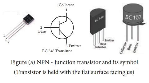
Figure
(a) NPN - Junction transistor and its symbol (Transistor is held with the flat
surface facing us)
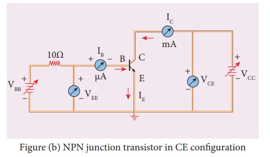
Figure
(b) NPN junction transistor in CE configuration
Note
A
resistor is connected in series with the base to prevent excess current flowing
into the base.
Precautions
┬Ę
Care should be taken to connect the
terminals of ammeters, voltmeters, and dc power supplies with right polarity.
┬Ę
The collector and emitter terminals of
the transistor must not be interchanged.
PROCEDURE
┬Ę
The connections are given as shown in
the diagram.
┬Ę
The current and voltage at the input and
output regions can be varied by adjusting the DC power supply.
i) Input characteristic curve: VBE vs IB (VCE constant)
┬Ę
The collector-emitter voltage VCE
is kept constant.
┬Ę
The base-emitter voltage VBE
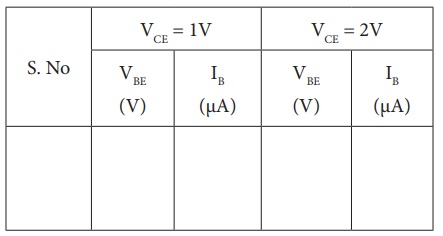
is varied in steps of 0.1V and the corresponding base current (IB)
is noted. The readings are taken till VCE reaches a constant value.
┬Ę
The same procedure is repeated for
different values of VCE. The readings are tabulated.
┬Ę
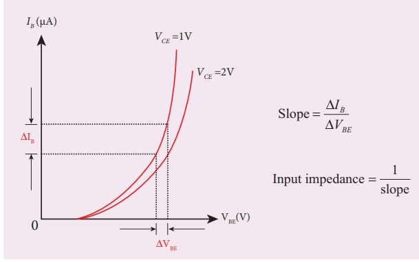
A graph is plotted by taking VBE along
x-axis and IB along y-axis for both the values of VCE.
┬Ę
The curves thus obtained are called the
input characteristics of a transistor.
┬Ę
The reciprocal of the slope of these
curves gives the input impedance of the transistor.
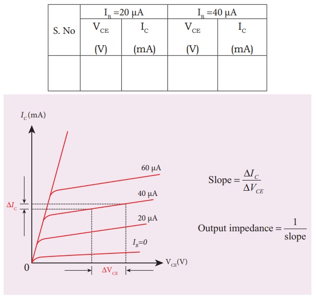
ii )Output characteristic curve: VCE vs IC (IB constant)
┬Ę
The base current IB is kept
constant.
┬Ę
VCE is varied in steps of 1V
and the corresponding collector current IC is noted. The readings
are taken till the collector current becomes almost constant.
┬Ę
Initially IB is kept at 0 mA
and the corresponding collector current is noted. This current is the reverse
saturation current ICEO.
┬Ę
The experiment is repeated for various
values of IB. The readings are tabulated.
┬Ę
A graph is drawn by taking VCE
along x-axis and IC along y-axis for various values of IB.
┬Ę
The set of curves thus obtained is
called the output characteristics of a transistor.
┬Ę
The reciprocal of the slope of the curve
gives output impedance of the transistor.
iii) Transfer characteristic curve: IB vs IC (VCE constant)
┬Ę
The collector-emitter voltage VCE
is kept constant.
┬Ę
The base current IB is varied
in steps of 10 ┬ĄA and the corresponding collector current IC is
noted.
┬Ę
This is repeated by changing the value
of VCE. The readings are tabulated.
┬Ę
The transfer characteristics is a plot
between the input current IB along x-axis and the output current IC
along y-axis keeping VCE constant.
┬Ę
The slope of the transfer
characteristics plot gives the current gain ╬▓ can be calculated.

RESULT
i)
The input, output and transfer characteristics of the NPN junction in common
emitter mode are drawn.
ii)
(a)
Input impedance = ________╬®
(b)
Output impedance = ________╬®
(c)
Current gain ╬▓ = ____(no unit)
Related Topics