Chapter: Digital Principles and System Design : Memory and Programmable Logic
Read Only Memory(ROM)
READ-ONLY MEMORY
A ROM is
essentially a memory device in which permanent binary information is stored.
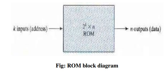
The inputs provide the address for memory and the
outputs give the data bits of the stored word that is selected by the address.
The number of words in a ROM is determined from the fact that k address input
lines are needed to specify 2k words.
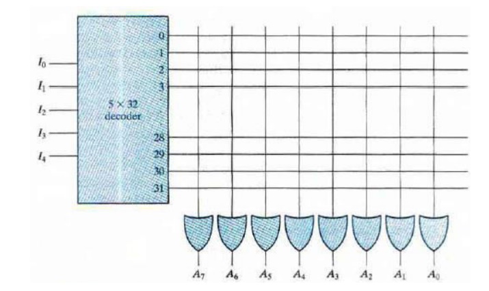
Fig:
Internal logic of a 32× 8 ROM ×
The five inputs are decoded into
32 distinct outputs by means of a 5 32 decoder. Each output of the decoder
represents a memory address. The 32 outputs of the decoder are connected to
each of the eight OR gates. Each OR gate must be considered as having 32
inputs. Each output of the decoder is connected to one of the inputs of each OR
gate. Since each OR gate has 32 input connections and there are 8 OR gates, the
ROM contains 32 x 8 = 256 internal connections.
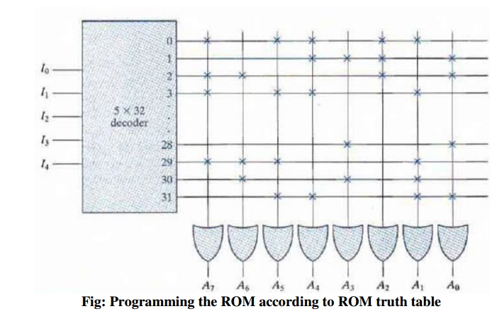
A programmable connection between two lines is
logically equivalent to a switch that can be altered to be either closed
(meaning that the two lines are connected) or open (meaning that the two lines
are disconnected). The programmable intersection between two lines is sometimes
called a cross point.
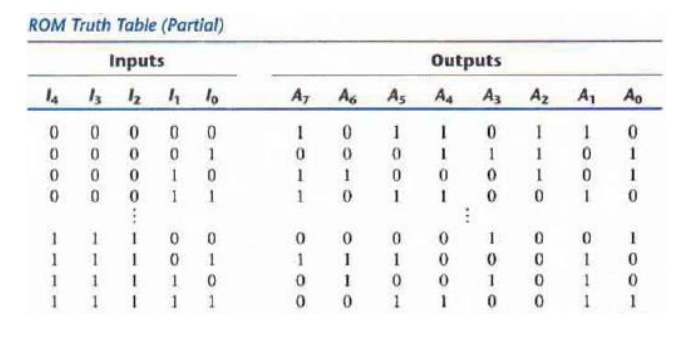
For example, programming the ROM according to the
truth table given by table. Every 0 listed in the truth table specifies the
absence of a connection and every 1 listed specifies a path that is obtained by
a connection.
Types of ROMs
The required paths in a ROM may be programmed in four
different ways.
ü
The first is called mask programming and is
done by the semiconductor company during the last fabrication process of the
unit. This procedure is costly because the vendor charges the customer a
special fee for custom masking the particular ROM.
ü
For small quantities, it is more economical to use
a second type of ROM called programmable read-only memory- PROM.
The fuses in the PROM are blown by the application of a high-voltage pulse
to the device through a special pin. A blown fuse defines a binary 0 state and
an intact fuse gives a binary 1 state. The hardware procedure for programming
ROMs or PROMs is irreversible and once programmed, the fixed pattern is
permanent and cannot be altered.
ü
A third type of R OM is the erasable PROM or
EPROM, which can be restructured to the initial state even though it has
been programmed previously. When the EPROM is placed under a special
ultraviolet light for a given length of time. the shortwave radiation
discharges the intern al floating gates that serve as the programmed
connections. After erasure, the EPROM returns to its initial state and can be
reprogrammed to a new set of values.
The fourth type of ROM is the electrically
erasable PROM (EEPROM or E2PROM). This device is like the EPROM
except that the previously programmed connections can be erased with an electrical
signal instead of ultraviolet light. The advantage is that the device can be
erased without removing it from its socket.
ü Flash
memory devices are similar to
EEPROMs, but have additional built-in circuitry to selectively program and erase the device
in-circuit, without the need for a special programmer. They have widespread
application in modern technology in cell phones, digital cameras, set-top
boxes, digital TV, telecommunications, non volatile data storage and
microcontrollers. Their low consumption of power makes them an attractive
storage medium for laptop and notebook computers.
Combinational PLDs
The PROM is a combinational programmable
logic device (PLD)-an integrated circuit with programmable gates divided into
an AND array and an OR array to provide an AND-OR sum of-product
implementation.
ü
There are three major types of combinational PLDs,
differing in the placement of the programmable connections in the AND-OR array.
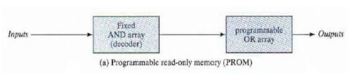
The PROM has a fixed AND array
constructed as a decoder and a programmable OR array. The programmable OR gates
implement the Boolean functions in sum-of-mintenns form.
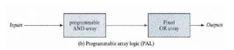
The PAL has a programmable AND
array and a fixed OR array. The AND gates are programmed to provide the product
terms for the Boolean functions, which are logically summed in each OR gate.
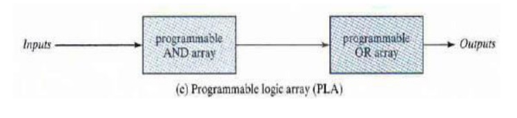
The most flexible PLD is the PLA, in which both the AND and OR
arrays can be programmed. The product terms in the AND array may be shared by
any OR gate to provide the required sum-of-products implementation.
Related Topics