Chapter: Digital Principles and System Design : Memory and Programmable Logic
Memory Decoding
MEMORY DECODING
In addition to requiring storage components in a memory unit,
there is a need for decoding circuits to select the memory word specified by
the input address.
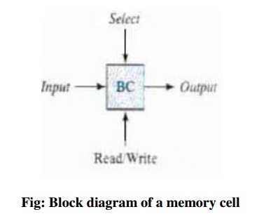
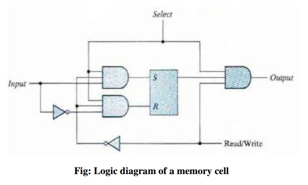
The storage part of the cell is modeled by an SR latch with
associated gate s to form a D latch. Actually, the cell is an electronic
circuit with four to six transistors. The select input enables the cell for
reading or writing and the read/write input determines the operation of the
cell when it is selected. A 1 in the read/write input provides the read
operation by fanning a path from the latch to the output terminal. A 0 in the
read/write input provides the write operation by forming a path from the input
terminal to the latch.
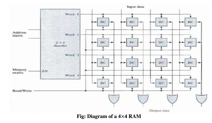
The logical construction of a
small RAM consists of four words of four bits each and bas a×total of 16 binary cells.
The small blocks labeled BC represent the binary cell with its three inputs and
one output. A memory with four words needs two address lines. The two address
inputs go through a 2 4 decoder to select one of the four words. The decoder is
enabled with the memory-enable input.
When the memory enable is 0, all
outputs of the decoder are 0 and none of the memory words are selected. With
the memory select at 1, one of the four words is selected, dictated by the
value in the two address lines.
Once a word has been selected,
the read/write input determines the operation. During the read operation the
four bits of the selected word go through OR gates to the output terminals.
During the write operation, the
data available in the input lines arc transferred into the four binary cells of
the selected word. The binary cells that are not selected are disabled and
their previous binary values remain unchanged.
When the memory select input that goes into the decoder is
equal to 0 none of the words are selected and the contents of all cells remain
unchanged regardless of the value of the read/write input.
ü
Coincident Decoding
A decoder with k inputs and 2k outputs
requires 2k AND gates with k inputs per gate. The total
number of gates and the number of inputs per gate can be reduced by employing
two decoders in a two - dimensional selection scheme.
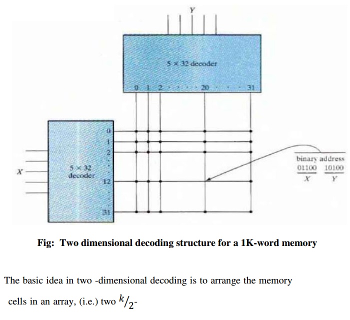
input decoders are used instead of one k-input decoder. One
decoder performs the row selection and the other the column selection in a
two-dimensional matrix configuration.
For example, instead of using a single 10 x 1,024 decoder, we
use two 5 x 32 decoders. With the single decoder, we would need 1,024 AND gates
with 10 inputs in each. The five most significant bits of the address go to
input X and the five least significant bits go to input Y. Each word within the
memory array is selected by the coincidence of one X line and one Y line. Thus
each word in memory is selected by the coincidence between 1 of 32 rows and 1
of 32 columns, for a total of 1,024 words.
ü
Address Multiplexing
Because of large capacity, the address decoding of DRAM is
arranged in a two dimensional array and larger memories often have multiple
arrays. To reduce the number of pins in the IC package, designers utilize
address multiplexing whereby one set of address input pins accommodates the
address components.
In a two-dimensional array, the address is applied in two
parts at different times, with the row address first and the column address
second. Since the same set of pins is used for both parts of the address, the
size of the package is decreased significantly.
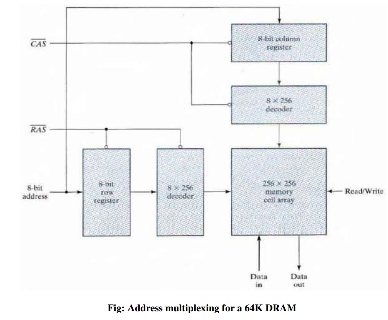
The memory consists of a two-dimensional array of cells
arranged into 256 rows by 256 columns, for a total of 28 x 28
= 216 = 64K words. There is a single data input line; a single data
output line, and a read/write control as well as an eight-bit address input and
two address strobes, the latter included for-enabling the row and column
address into their respective registers. The row address strobe (RAS) enables
the eight-bit row register and the column address strobe (CAS) enables the
eight-bit column register. The bar on top of the name of the strobe symbol
indicates that the registers are enabled on the zero level of the signal.
Related Topics