Chapter: High Voltage Engineering : Generation of High Voltages and High Currents
Half Wave Rectifier Circuit - Generation of High Voltages and Currents
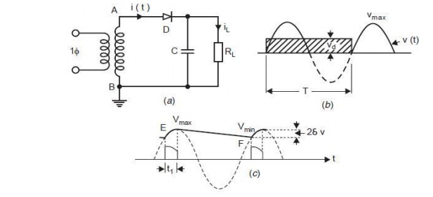
Half Wave Rectifier Circuit
The
simplest circuit for generation of high direct voltage is the half wave
rectifier shown in Fig. 3.1 Here RL is the load resistance and C the
capacitance to smoothen the dace. output voltage. If the capacitor is not
connected, pulsating dace. voltage is obtained at the output terminals where as
with the capacitance C, the pulsation at the output terminal are reduced.
Assuming the ideal transformer and small internal resistance of the diode
during conduction the capacitor C is charged to the maximum voltage Vmax
during conduction of the diode D. Assuming that there is no load connected, the
dace. Voltage across capacitance remains constant at Vmax whereas
the supply voltage oscillates between ± Vmax and during negative
half cycle the potential of point A becomes – Vmax and hence the
diode must be rated for 2Vmax. This would also be the case if the transformer
is grounded at A instead of B as shown in Fig. 3.1 (a). Such a circuit is known
as voltage doublers due to Villard for which the output voltage would be taken
across D. This dace. voltage, however, oscillates between zero and 2Vmax and is
needed for the Cascade circuit.
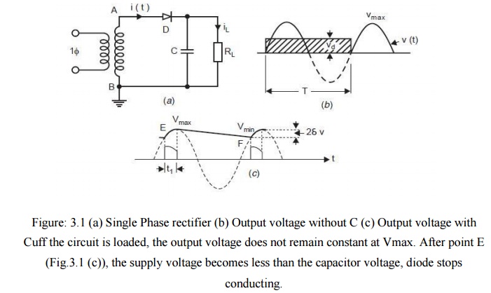
Figure:
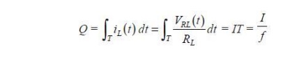
3.1 (a) Single Phase rectifier (b) Output voltage without C (c) Output voltage
with Cuff the circuit is loaded, the output voltage does not remain constant at
Vmax. After point E (Fig.3.1 (c)), the supply voltage becomes less than the
capacitor voltage, diode stops conducting.
The
capacitor cannot discharge back into the a.c. system because of one way action
of the diode. Instead, the current now flows out of C to furnish the current
ill through the load. While giving up this energy, the capacitor voltage also
decreases at a rate depending on the time constant CR of the circuit and it
reaches the point F corresponding to V min. Beyond F, the supply voltage is
greater than the capacitor voltage and hence the diode D starts conducting
charging the capacitor C again to Vmax and also during this period it supplies
current to the load also. This second pulse of imp(ic + il) is of shorter
duration than the initial charging pulse as it serve mainly to restore into C
the energy that C meanwhile had supplied to load. Thus, while each pulse of
diode current lasts much less than a half cycle, the load receives current more
continuously from C. Assuming the charge supplied by the transformer to the
load during the conduction period t, which is very small to be negligible, the
charge supplied by the transformer to the capacitor during conduction equals
the charge supplied by the capacitor to the load. Note that ic>> iL.
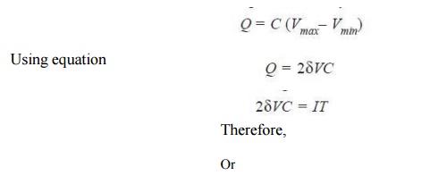
During one period T = 1/f of the a.c voltage, a charge Q is transferred to the
load RL and is given as
where I
is the mean value of the dace output iL(t) and VRL(t) the dace. voltage which
includes a ripple as shown in Fig. 2.1 (c). This charge is supplied by the
capacitor over the period T when the voltage changes from Vmax to Vmin over
approximately period T neglecting the conduction period of the diode. Suppose
at any time the voltage of the capacitor is V and it decreases by an amount of
dV over the time dt then charge delivered by the capacitor during this time is

Therefore,
if voltage changes from Vmax to Vmin, the charge delivered by the capacitor
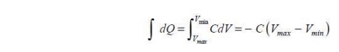
Or the
magnitude of charge delivered by the capacitor
The above
equation shows that the ripple in a rectifier output depends upon the load
current and the circuit parameter like f and C. The product fC is, therefore,
an important design factor for the rectifiers. The higher the frequency of
supply and larger the value of filtering capacitor the smaller will be the
ripple in the dace. output. The single phase half-wave rectifier circuits have
the following disadvantages:
·
The size of the circuits is very large if high and
pure dace. output voltages are desired.
· The h.t. transformer may get saturated if the amplitude of direct current is comparable with the nominal alternating current of the transformer.
It is to
be noted that all the circuits considered here are able to supply relatively
low currents and therefore are not suitable for high current applications such
as HVDC transmission. When high dace. voltages are to be generated, voltage
doubler or cascaded voltage multiplier circuits are used. One of the most
popular doubler circuit due to Greinacher is shown in Fig. 3.2. Suppose B is
more positive with respect to A and the diode D1 conducts thus
charging the capacitor C1 to Vmax with polarity as shown in Fig.
3.2. During the next half cycle terminal A of the capacitor C1 rises
to Vmax and hence terminal M attains a potential of 2 Vmax. Thus, the capacitor
C2 is charged to 2 Vmax through D2. Normally the voltage
across the load will be less than 2 Vmax depending upon the time constant of
the circuit C2RL.
Related Topics