Chapter: Linear Integrated Ciruits : Characteristics of op-amp
General Operational Amplifier
General Operational Amplifier:
An
operational amplifier generally consists of three stages, anmely,1. a
differential amplifier 2. additional amplifier stages to provide the required
voltage gain and dc level shifting 3. an emitter-follower or source follower
output stage to provide current gain and low output resistance.
A
low-frequency or dc gain of approximately 104 is desired for a
general purpose op-amp and hence, the use of active load is preferred in the
internal circuitry of op-amp. The output voltage is required to be at ground,
when the differential input voltages is zero, and this necessitates the use of
dual polarity supply voltage. Since the output resistance of op-amp is required
to be low, a complementary push-pull emitter – follower or source follower
output stage is employed. Moreover, as the input bias currents are to be very
small of the order of picoamperes, an FET input stage is normally preferred.
The figure shows a general op-amp circuit using JFET input devices.
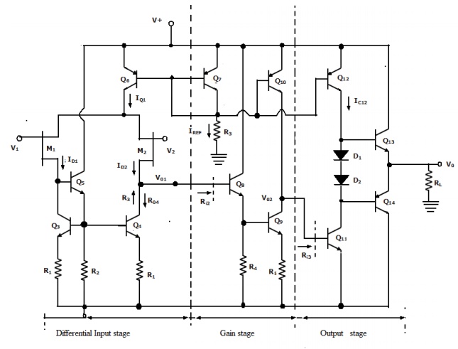
Input stage:
The input
differential amplifier stage uses p-channel JFETs M1 and M2. It employs a
three-transistor active load formed by Q3 , Q4 , and Q5 . the bias current for
the stage is provided by a two-transistor current source using PNP transistors
Q6 and Q7. Resistor R1 increases the output resistance seen looking into the
collector of Q4 as indicated by R04. This is necessary to provide bias current
stability against the transistor parameter variations. Resistor R2 establishes
a definite bias current through Q5 . A single ended output is taken out at the
collector of Q4 .
MOSFET‘s
are used in place of JFETs with additional devices in the circuit to prevent
any damage for the gate oxide due to electrostatic discharges.
Gain stage:
The
second stage or the gain stage uses Darlington transistor pair formed by Q8 and
Q9 as shown in figure. The transistor Q8 is connected as an emitter follower,
providing large input resistance.
Therefore,
it minimizes the loading effect on the input differential amplifier stage. The
transistor Q9 provides an additional gain and Q10 acts as an active load for
this stage. The current mirror formed by Q7 and Q10 establishes the bias
current for Q9 . The VBE drop across Q9 and drop across R5 constitute the
voltage drop across R4 , and this voltage sets the current through Q8 . It can
be set to a small value, such that the base current of Q8 also is very less.
Output stage:
The final
stage of the op-amp is a class AB complementary push-pull output stage. Q11 is
an emitter follower, providing a large input resistance for minimizing the
loading effects on the gain stage. Bias current for Q11 is provided by the
current mirror formed by Q7 and Q12, through Q13 and Q14 for minimizing the
cross over distortion. Transistors can also be used in place of the two diodes.
The
overall voltage gain AV of the op-amp is the product of voltage gain of each
stage as given by AV = |Ad | |A2 ||A3 |
Where Ad
is the gain of the differential amplifier stage, A2 is the gain of the second
gain stage and A3 is the gain of the output stage.
Related Topics