Chapter: Electronic Devices : Special Semiconductor Devices
Zener diode
ZENER DIODE
A Zener
diode is a t ype of diode that permits current not only in the forward
direction like a normal diode, but also in the reverse direction if the voltage
is lar ger than the breakdown voltage known as "Zener knee voltage"
or "Zener voltage". The device was named after Clarence Zener, who
discovered this el ectrical property.
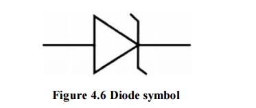
Figure 4.6 Diode symbol
However,
the Zener Diode or "Breakdown Diode" as they are sometimes called,
are basically the same as the standard PN junction diode but are specially designed
to have a low pre-determined Reverse Brea kdown Voltage that takes advantage of
this high reverse voltage. The point at which a zener dio de breaks down or
conducts is called the "Ze ner Voltage" (Vz).
The Zener
diode is like a general-purpose signal diode consisting of a silicon PN
junction. When biased in the forward direction it behaves just like a nor mal
signal diode passing the rated current, but when a reverse voltage is applied
to it the reverse saturation current remains fairly constant over a wide range
of voltages. The reverse vo ltage increases until the
diodes
breakdown voltage V B is reached at which point a process called Avalanche
Breakdown occurs in the depletion lay er and the current flowing through the
zener diode increases dramatically to the maximum circuit value (which is
usually limited by a series resistor). This breakdown voltage point is called
the "zener voltage" for zener diodes.
Avalanche
Breakdo wn: There is a limit for the reverse voltag e. Reverse voltage can increase
until the diode brea kdown voltage reaches. This point is called Avalanche
Breakdown region. At this stage maximu m current will flow through the zener
diode. This breakdown point is referred as “Zener voltage”.
The point at which current flows can be very
accurately cont rolled (to less than 1% tolerance) in the doping st age of the
diodes construction giving the diode a specific zener breakdown voltage, (Vz)
ra nging from a few volts up to a few hundred volts. This zener breakdown
voltage on the I-V curve is almost a vertical straight line.
Zener diode characteristics
The Zener
Diode is used in its "reverse bias" or reverse breakdo wn mode, i.e.
the diodes anode connects to the negativ e supply. From the I-V characteristics
curv e above, we can see that the zener diode has a regio n in its reverse bias
characteristics of almost a constant negative voltage regardless of the value
of the current flowing through the di ode and remains nearly constant even with
large cha nges in current as long as the zener diodes current remains between
the breakdown current IZ(min) and the maximum current rating IZ(max).
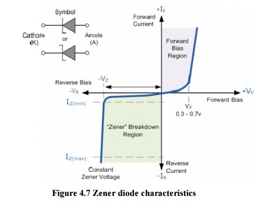
Figure 4.7 Zener diode characteristics
Applications of zener diode
1.The Zener Diode Regulator
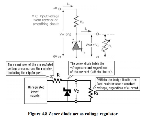
Figu re 4.8 Zener diode act as
voltage regulator
The
constant reverse voltage ![]()
![]() of the zener diode makes it a valua ble
component for the regulation of the output voltagge against both variations in
the input volta ge from an unregulated power supply or variations in t he load
resistance. The current through the ze ner will change to keep the voltage at
within the limit s of the threshold of zener action and the maximum power it
can dissipate.
of the zener diode makes it a valua ble
component for the regulation of the output voltagge against both variations in
the input volta ge from an unregulated power supply or variations in t he load
resistance. The current through the ze ner will change to keep the voltage at
within the limit s of the threshold of zener action and the maximum power it
can dissipate.
2. Zener-Controlled Output Switching
This
comparator application makes use of the properties of the zener diode to cause
the output to switch between voltages determined by the zener diodes when the
input voltage difference ![]()
![]()
![]()
![]()
![]() changes sign. The output circuit amounts to a
zener regulator which switches from one zener voltage to the other on a
transition.
changes sign. The output circuit amounts to a
zener regulator which switches from one zener voltage to the other on a
transition.
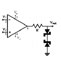
3. Zener Limiter
A single
Zener diode can limit one side of a sinusoidal waveform to the zener voltage
while clamping the other side to near zero. With two opposing zeners, the
waveform can be limited to the zener voltage on both polarities.
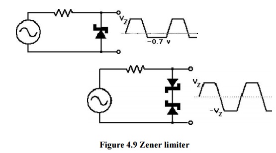
Figure 4.9 Zener limiter
4. Zener Role in Power Supplies
The zener
diode is widely used as a voltage regulator because of its capacity to maintain
a constant voltage over a sizeable range of currents. It can be used as a
single component across the output of a rectifier or incorporated into one of
the variety of one-chip regulators Basically there are two type of regulations
such as:
a) Line Regulation
In this
type of regulation, series resistance and load resistance are fixed, only input
voltage is changing. Output voltage remains the same as long as the input
voltage is maintained above a
minimum
value.
Percentage of line regulation can be calculated by =
Where V0
is the output voltage and VIN is the input voltage and ΔV0
is the change in output voltage for a particular change in input voltage ΔVIN.
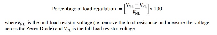
b) Load Regulation
In this
type of regulation, input voltage is fixed and the load resistance is varying.
Output volt remains same, as long as the load resistance is maintained above a
minimum value.
Difference between Zener breakdown from avalanche
breakdown
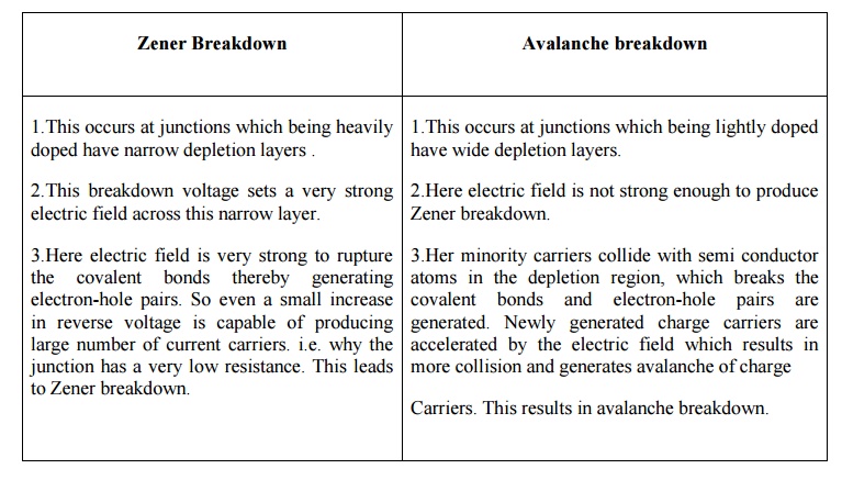
Zener Breakdown
1.This
occurs at junctions which being heavily doped have narrow depletion layers .
2.This
breakdown voltage sets a very strong electric field across this narrow layer.
3.Here
electric field is very strong to rupture the covalent bonds thereby generating
electron-hole pairs. So even a small increase in reverse voltage is capable of
producing large number of current carriers. i.e. why the junction has a very
low resistance. This leads to Zener breakdown.
Avalanche breakdown
1.This
occurs at junctions which being lightly doped have wide depletion layers.
2.Here
electric field is not strong enough to produce Zener breakdown.
3.Her
minority carriers collide with semi conductor atoms in the depletion region,
which breaks the covalent bonds and electron-hole pairs are generated. Newly
generated charge carriers are accelerated by the electric field which results in
more collision and generates avalanche of charge Carriers. This results in
avalanche breakdown.
Related Topics