Chapter: Electronic Devices : Special Semiconductor Devices
Schottky Barrier (Hot-Carrier) Diodes
SCHOTTKY BARRIER (HOT-CARRIER) DIODES
A Schottky diode, also known as a hot carrier
diode, is a semiconductor diode which has a low forward voltage drop and a very
fast switching action. There is a small voltage drop across the diode terminals
when current flows through a diode.
A normal
diode will have a voltage drop between 0.6 to 1.7 volts, while a Schottky diode
voltage drop is usually between 0.15 and 0.45 volts. This lower voltage drop
provides better system efficiency and higher switching speed.
In a Schottky diode, a semiconductor–metal junction
is formed b etween a semiconductor and a metal, thus creating a Schottky
barrier. The N-type semiconductor acts as the cathode and the metal side acts
as the ano de of the diode. This Schottky barrier result s in both a low
forward voltage drop and very fast swiitching.
1 Symbol and Construction
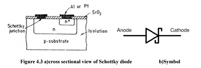
It can be
seen from the circuit symbol that it is based on the nor mal diode one, but
with additional elements to the bar a cross the triangle shape.
Its construction is quite different from the
conventional p-n junction in that a metalsemiconductor j u n c t i o n is
created such as shown in Figure 4.3 . The semiconductor is normally n-type
silicon (although p-type silicon is sometimes used), w hiles a host of
different metals, such as molybdenum, platinum, chrome, or tungsten, are used.
Different construction techniques will result in a
different set of characteristics for the device, such as increased freq uency
range, lower forward bias, and so on. Priorities do not permit an examination
of each te chnique here, but information will usuall y be provided by the
manufacturer. In general, how ever, Schottky diode construction results in a
more uniform junction region and a high level of rug gedness.
In both
materials, the electron is the majority carrier. In the met al, the level of
minority carriers (holes) is insignifican t. When the materials are joined, the
electr ons in the n-type silicon semiconductor material immediately flow into
the adjoining metal, estab lishing a heavy flow of majority carriers. Since the
injected carriers have a very high kinetic en ergy level compared to the
electrons of the metal, the y are commonly called ―hot carriers.
The
additional carrie rs in the metal establish a ―negative wall in the metal at
the boundary between the two materials. The net result is a ―surface barrier
betw een t h e two materials, preventing any further curr ent. That is, any
electrons (negatively charged) in the silicon material face a carrier-free
regio n and a ―negative wall at the surface of the metal.
The
application of a forward bias as shown in the first quadrant o f Figure 4.2
will reduce the strength of the negative barrier through the attraction of the
applied positive potential for electrons from this regi on. The result is a
return to the heavy f low of electrons across the boundary, the magnitude of
which is controlled by the level of the app lied bias potential.
The
barrier at the junc tion for a Schottky diode is less than that of the p-n
junction device in both the forward- and re verse-bias regions. The result is
therefore a higher current at the same applied bias in the forward- and
reverse-bias regions. This is a desirable effect in the forward-bias region but
highl y undesirable in the reverse-bias region.
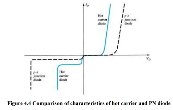
Figure 4.4 Comparison of
characteristics of hot carrier and PN diode
Advantages
Schottky
diodes are used in many applications where other types of diode will not
perform as well. They offer a number of advantages:
·
Low turn on voltage: The turn on voltage for the
diode is between 0.2 and 0.3 volts for a silicon diode against 0.6 to 0.7 volts
for a standard silicon diode. This makes it have very much the same turn on
voltage as a germanium diode.
·
Fast recovery time: The fast recovery time because
of the small amount of stored charge means that it can be used for high speed
switching applications.
·
Low junction capacitance: In view of the very small
active area, often as a result of using a wire point contact onto the silicon,
the capacitance levels are very small.
The
advantages of the Schottky diode, mean that its performance can far exceed that
of other diodes in many areas.
Applications
The
Schottky barrier diodes are widely used in the electronics industry finding
many uses as diode rectifier. Its unique properties enable it to be used in a
number of applications where other diodes would not be able to provide the same
level of performance. In particular it is used in areas including:
·
RF mixer
and detector diode: The Schottky diode has come into its own for radio frequency applications because of its
high switching speed and high frequency capability. In view of this Schottky
barrier diodes are used in many high performance diode ring mixers. In addition
to this their low turn on voltage and high frequency capability and low
capacitance make them ideal as RF detectors.
Power rectifier: Schottky barrier diodes are also
used in high power applications, as rectifiers.
Their high current density and low forward voltage drop mean that less power is
wasted than if ordinary PN junction diodes were used. This increase in
efficiency means that less heat has to be dissipated, and smaller heat sinks
may be able to be incorporated in the design.
·
Power OR
circuits: Schottky diodes can be used in applications where a load is driven by two separate power supplies. One
example may be a mains power supply and a battery supply. In these instances it
is necessary that the power from one supply does not enter the other. This can
be achieved using diodes. However it is important that any voltage drop across
the diodes is minimised to ensure maximum efficiency. As in many other
applications, this diode is ideal for this in view of its low forward voltage
drop. Schottky diodes tend to have a high reverse leakage current. This can
lead to problems with any sensing circuits that may be in use. Leakage paths
into high impedance circuits can give rise to false readings. This must
therefore be accommodated in the circuit design.
·
Solar
cell applications: Solar cells are typically connected to rechargeable
batteries, often lead acid batteries
because power may be required 24 hours a day and the Sun is not always
available. Solar cells do not like the reverse charge applied and therefore a
diode is required in series with the solar cells. Any voltage drop will result
in a reduction in efficiency and therefore a low voltage drop diode is needed.
As in other applications, the low voltage drop of the Schottky diode is
particularly useful, and as a result they are the favoured form of diode in
this application.
· Clamp diode - especially with its use in LS TTL: Schottky barrier diodes may also be used as a clamp diode in a transistor circuit to speed the operation when used as a switch. They were used in this role in the 74LS (low power Schottky) and 74S (Schottky) families of logic circuits. In these chips the diodes are inserted between the collector and base of the driver transistor to act as a clamp. To produce a low or logic "0" output the transistor is driven hard on, and in this situation the base collector junction in the diode is forward biased. When the Schottky diode is present this takes most of the current and allows the turn off time of the transistor to be greatly reduced, thereby improving the speed of the circuit.
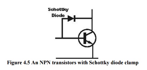
Figure 4.5 An NPN transistors
with Schottky diode clamp
In view
of its properties, the Schottky diode finds uses in applications right through
from power rectification to uses in clamp diodes in high speed logic devices
and then on to high frequency RF applications as signal rectifiers and in
mixers.
Their
properties span many different types of circuit making them almost unique in
the variety of areas and circuits in which they can be used.
Related Topics