Chapter: Electronic Devices : Special Semiconductor Devices
Metal-Semiconductor Field Effect Transistor (MESFETs)
Metal-Semiconductor Field Effect Transistor
(MESFETs)
MESFET
stands for metal–semiconductor field effect transistor. It is quite similar to
a JFET in construction and term inology. The difference is that instead of
using a p-n junction for a gate, a Schottky (metal-semiconductor) junction is
used. MESFETs are usually constructed in compound semiconductor technologies
lacking high quality surface passivation such as GaAs, InP, or SiC, and are
faster but m ore expensive than silicon-based JFETs or MOSFETs. Production
MESFETs are operated up to approximately 45 GHz, and are commonly used for
microwave frequency communications an d radar. From a digital circuit design
perspe ctive, it is increasingly difficult to use MESFETs as th e basis for
digital integrated circuits as the s cale of integration goes up, compared to
CMOS silicon based fabrication.
The
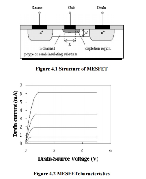
Metal-Semiconductor-Field-Effect-Transistor (MESFET) co nsists of a conducting
channel positioned between a source and drain contact region as shown in the
Figure 4.1. The carrier flow from source to drain is controlled by a Schottky
metal gate. The control of the channel is obtained by varying the deplletion
layer width underneath the metal conta ct which modulates the thickness of the
conducting ch annel and thereby the current between source and drain.

Figure 4.2 MESFETcharacteristics
Application
Numerous
MESFET fabrication possibilities have been explored for a wide variety of
semiconductor systems. Some of the main application areas are:
·
military communications
·
As front end low noise amplifier of microwave
receivers in both military radar devices and communication
·
commercial optoelectronics
·
satellite communications
·
As power amplifier for output stage of microwave
links.
·
As a power oscillator.
Advantage of the MESFET
·
The higher transit frequency of the MESFET makes it
particularly of interest for microwave circuits. While the advantage of the
MESFET provides a superior microwave amplifier or circuit, the limitation by
the diode turn-on is easily tolerated.
·
Typically depletion-mode devices are used since
they provide a larger current and larger transconductance and the circuits
contain only a few transistors, so that threshold control is not a limiting
factor.
·
The buried channel also yields a better noise
performance as trapping and release of carriers into and from surface states
and defects is eliminated.
·
The use of GaAs rather than silicon MESFETs
provides two more significant advantages: first, the electron mobility at room
temperature is more than 5 times larger, while the peak electron velocity is
about twice that of silicon.
·
Second, it is possible to fabricate semi-insulating
(SI) GaAs substrates, which eliminates the problem of absorbing microwave power
in the substrate due to free carrier absorption.
Disadvantage of the MESFET
·
The disadvantage of the MESFET structure is the
presence of the Schottky metal gate. It limits the forward bias voltage on the
gate to the turn-on voltage of the Schottky diode. This turn-on voltage is
typically 0.7 V for GaAs Schottky diodes.
·
The threshold voltage therefore must be lower than
this turn-on voltage. As a result it is more difficult to fabricate circuits
containing a large number of enhancement-mode
MESFET.
Related Topics