Chapter: Basic Electrical and electronics : Semiconductor Devices And Applications
Zener Diode
ZENER EFFECT
Ø In a general
purpose PN diode the doping is light; as a result of this the breakdown voltage
is high. If a P and N region are heavily doped then the breakdown voltage can
be reduced.
Ø When the
doping is heavy, even the reverse voltage is low, the electric field at barrier
will be so strong thus the electrons in the covalent bonds can break away from
the bonds. This effect is known as Zener
effect.
ZENER DIODE

Ø A diode
which exhibits the zener effect is called a Zener Diode. Hence it is defined as a reverse biased heavily doped
PN junction diode which operates in breakdown region. The zener diodes have
been designed to operate at voltages ranging from a few volts to several
hundred volts.
Ø Zener Breakdown occurs in junctions which is heavily
doped and have narrow depletion layers.
The breakdown voltage sets up a very strong electric field. This field is so
strong enough to break or rupture the covalent bonds thereby generating
electron hole pairs.
Ø Even a
small reverse voltage is capable of producing large number of current carrier.
When a zener diode is operated in the breakdown region care must be taken to
see that the power dissipation across the junction is within the power rating
of the diode otherwise heavy current flowing through the diode may destroy it.
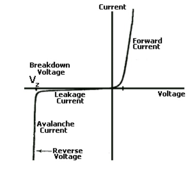
V-I characteristics of Zener diode

Ø The illustration above shows this
phenomenon in a current vs voltage graph with a zener diode connected in the
forward direction .It behaves exactly as a standard diode.
Ø In the
reverse direction however
there is a
very small leakage
current between 0v
and the
zener voltage –i.e. just a tiny amount of current is able to flow.
Ø Then,
when the voltage reaches the breakdown voltage (vz),suddenly current can flow
freely through it.
Application of Zener diode
a) as
voltage regulator
b) as peak
clippers
c) for
reshaping waveforms
Related Topics