Chapter: Basic Electrical and electronics : Semiconductor Devices And Applications
Bipolar Junction Transistor(BJT)
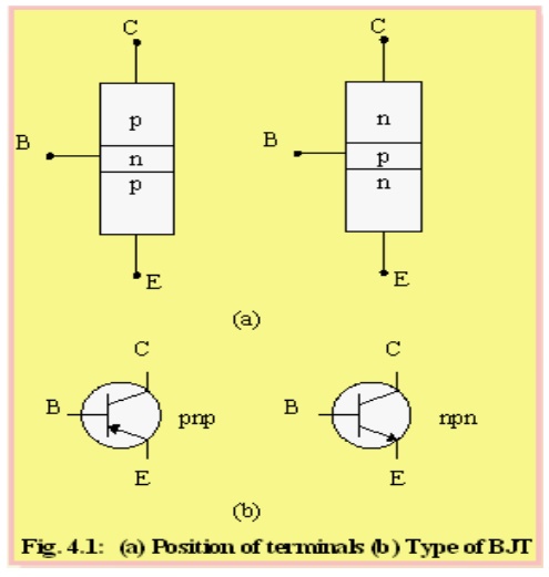
BIPOLAR JUNCTION TRANSISTOR
Ø A bipolar
junction transistor is a three terminal semiconductor device in which the
operation depends on the interaction of majority and minority carriers.
Ø Transistor
refers to Transfer Resistor i.e., signals are transferred from low resistance
circuit into high resistance circuit.
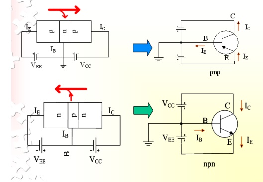
Ø BJT
consists of silicon crystal in which a layer of ‘N’ type silicon is sandwiched
between two layers of ‘P’ type silicon. The semiconductor sandwiched is
extremely smaller in size.
Ø In other
words, it consists of two back to back PN junction joined together to form
single piece of semiconductor crystal. These two junctions gives three region
called Emitter, Base and Collector.
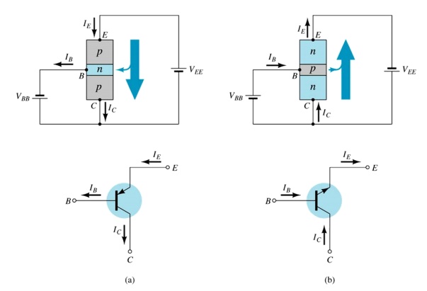
Ø There are
two types of transistors such as PNP and NPN. The arrow on the emitter
specifies whether the transistor is PNP or NPN type and also determines the
direction of flow of current, when the emitter base junction is forward biased.
Emitter: It is more heavily doped than any
of the other region because its main function is to supply majority charge carriers to the base.
Base: It forms the middle section of
the transistor. It is very thin as compared to either the emitter or collector and is very lightly doped.
Collector: Its main function is to collect
the majority charge carriers coming from the emitter and passing through the base. In most transistors, collector
region is made physically larger than the emitter because it has to dissipate
much greater power.
Operation of Transistor
Ø The basic
operation will be described using the pnp transistor. The operation of the pnp
transistor is exactly the same if the roles played by the electron and hole are
interchanged.
Ø One p-n
junction of a transistor is reverse-biased, whereas the other is
forward-biased.
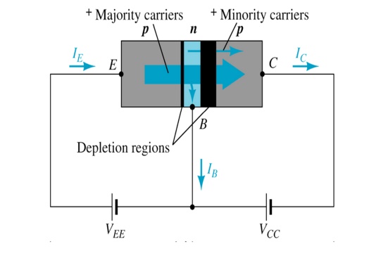
Ø Both
biasing potentials have been applied to a pnp transistor and resulting majority
and minority carrier flows indicated.
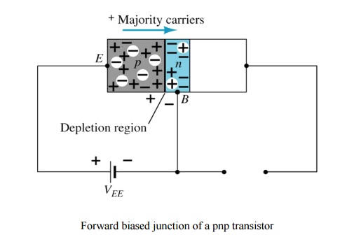
Ø Majority
carriers (+) will diffuse across the forward-biased p-n junction into the
n-type material.
Ø A very
small number of carriers (+) will through n-type material to the base terminal.
Resulting IB is typically in order of microamperes.
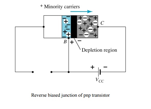
Ø The large
number of majority carriers will diffuse across the reverse-biased junction
into the p-type material connected to the collector terminal.
Ø Majority
carriers can cross the reverse-biased junction because the injected majority
carriers will appear as minority carriers in the n-type material.
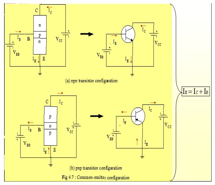
Ø Applying KCL to the transistor :
IE = IC + IB
Ø The comprises of two components – the
majority and minority carriers
IC = ICmajority + ICOminority
Ø ICO
– IC current with emitter terminal open and is called leakage
current.
Common Base configuration
Ø Common-base
terminology is derived from the fact that the :
-
base is common to both input and output of the
configuration.
-
base is usually the terminal closest to or at
ground potential.
Ø All current
directions will refer to conventional (hole) flow and the arrows in all
electronic symbols have a direction defined by this convention.
Ø Note that
the applied biasing (voltage sources) are such as to establish current in the
direction indicated for each branch.
Ø To
describe the behavior of common-base amplifiers requires two set of
characteristics: o Input or driving point characteristics.
o Output or collector
characteristics
Ø The
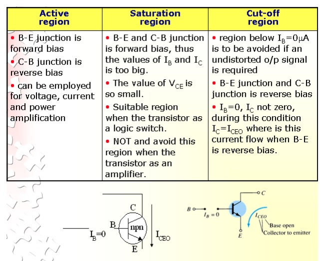
output characteristics has 3 basic regions:
o Active region –defined by the biasing
arrangements
o Cutoff region – region where the collector
current is 0A
o
Saturation
region- region of the characteristics to the left of VCB = 0V
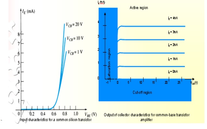
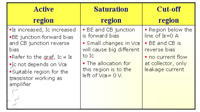
Ø The
curves (output characteristics) clearly indicate that a first approximation to
the relationship between IE and IC in the active region is given by
IC
≈IE
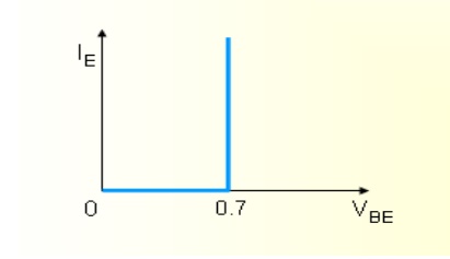
Ø Once a transistor is in the ‘on’ state, the
base-emitter voltage will be assumed to be
VBE
= 0.7V
Ø In the dc
mode the level of IC and IE due to the majority carriers
are related by a quantity called alpha
α = IC / IE
IC
= α IE + ICBO
Ø It can then be summarize to IC = αIE (ignore ICBO
due to small value)
Ø For ac
situations where the point of operation moves on the characteristics curve, an
ac alpha defined by
Ø Alpha a common base current gain factor that shows the efficiency by calculating the current percent from current flow from emitter to collector. The value of is typical from
0.9 ~
0.998.
Common Emitter configuration
Ø It is called common-emitter
configuration since :
o emitter is common or reference to both input
and output terminals.
o
emitter is usually the terminal closest to or at
ground potential.
Ø Almost
amplifier design is using connection of CE due to the high gain for current and
voltage.
Ø Two set
of characteristics are necessary to describe the behavior for CE; input (base
terminal) and output (collector terminal) parameters.
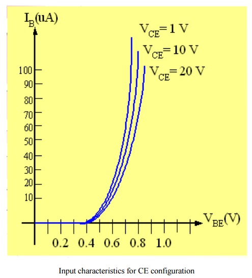
Input
characteristics for CE configuration
Ø IB
in microamperes compared to milliamperes of IC.
Ø IB
will flow when VBE > 0.7V for silicon and 0.3V for germanium
Ø Before
this value IB is very small and no IB.
Ø Base-emitter
junction is forward bias
Ø Increasing
VCE will reduce IB for different values.
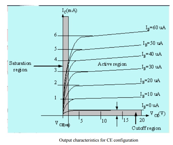
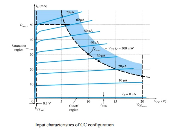
Output
characteristics for CE configuration
Ø For small
VCE (VCE < VCESAT, IC increase
linearly with increasing of VCE
Ø VCE
> VCESAT IC not totally depends on VCE -- > constant IC
Ø IB(uA)
is very small compare to IC (mA). Small increase in IB
cause big increase in IC
Ø IB=0
A -- > ICEO occur.
Ø Noticing
the value when IC=0A. There is still some value of current flows.
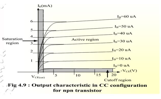
Common Collector configuration
Ø Also
called emitter-follower (EF).
Ø It is
called common-emitter configuration since both the
o
signal source and the load share the collector
terminal as a common connection point.
Ø The
output voltage is obtained at emitter terminal.
Ø The input
characteristic of common-collector configuration is similar with
common-emitter. configuration.
Ø Common-collector
circuit configuration is provided with the load resistor connected from emitter
to ground.
Ø It is
used primarily for impedance-matching purpose since it has high input impedance
and low output impedance.
Ø For the
common-collector configuration, the output characteristics are a plot of IE
vs VCE for a range of values of IB.
Small Signal Amplifier
When the
input signal is so weak as to produce small fluctuations in the collector
current compared to its quiescent value, the amplifier is known as Small Signal
Amplifier.
In other
words, as the name indicates, the input applied to the circuit is Vin
<< Vth. It has only one amplifying device.
Α = IC / IE
IC
= α
IE + ICBO
Voltage
and current equation for hybrid parameters:
V1
= h11i1 + h12V2
I2
= h21i1 + h22V2
The values
of h-parameters:
h11
= V1/ i1
h12
= V1 / V2
h21
= i2 / i1
h22 = i2 /
V2
Related Topics