Chapter: Electronic Circuits : BJT Amplifiers
Techniques of Improving Input Impedance
Techniques of Improving Input Impedance
Among three configurations (CB, CC and CE), common collector or emitter follower circuit has high input impedance. Typically it is 200 KΩ to 300 KΩ. A single stage emitter follower circuit can give input impedance upto 500 KΩ. However, the input impedance considering biasing resistors is
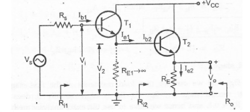
Figure shows the direct coupling of two stages of emitter follower significantly less. Because Ri’ = R1ll R2llRi The input impedance of the circuit can be improved by direct coupling of two stages of emitter follower amplifier. The input impedance can be increased using two techniques :
• Using direct coupling (Darlington connection)
• Using Bootstrap technique
1. Darlington Transistors
Figure shows the direct coupling of two stages of emitter follower amplifier. This cascaded connection of two emitter followers is called the Darlington connection
Assume that the load resistance RL is such that RL hoe < 0.1, therefore we can use approximate analysis method for analyzing second stage
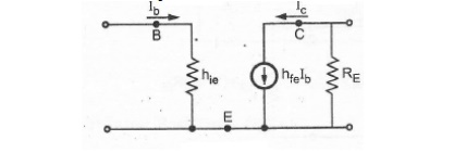
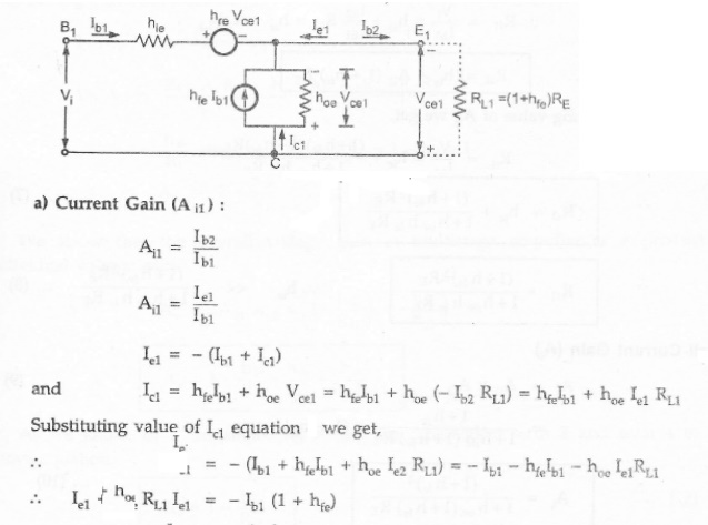
Figure shows approximate h-parameter (AC) equivalent circuit for common emitter configuration. The same circuit can be redrawn by making collector common to have approximate h-parameter equivalent circuit for common collector configuration.
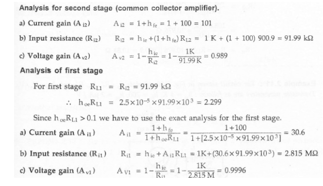
Analysis of Second stage :
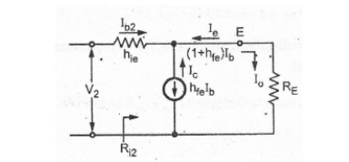
Analysis of first stage :
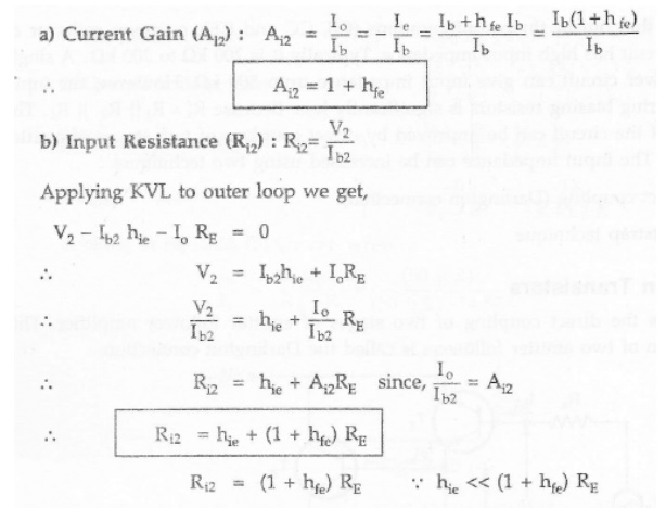
Load resistance of the first stage is the input resistance of the second stage i.e. Ri2. As Ri2 is high, usually it does not meet the requirement hoe Ri2< 0.1, and hence we have to use the exact analysis method for analysis of the first stage.
Figure shows the h-parameter equivalent circuit for common emitter configuration.
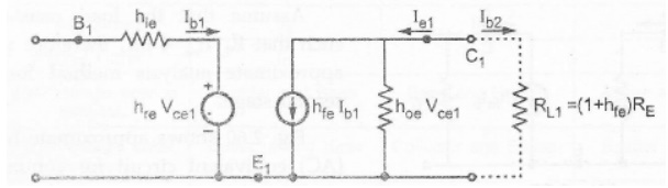
The same circuit can be redrawn by making collector common to have h-parameter equivalent circuit for common collector for configuration.
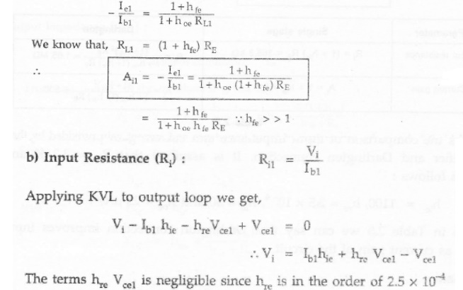
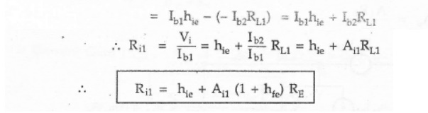
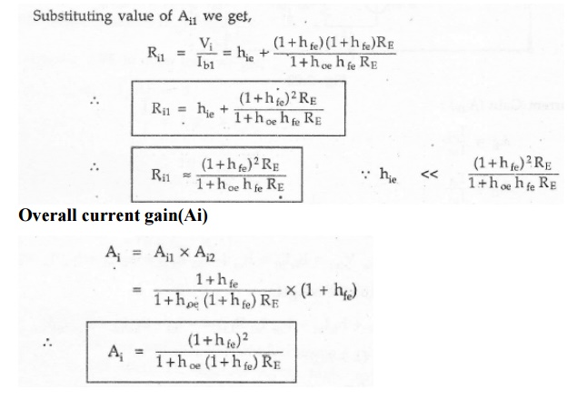
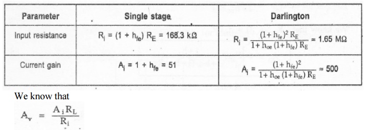
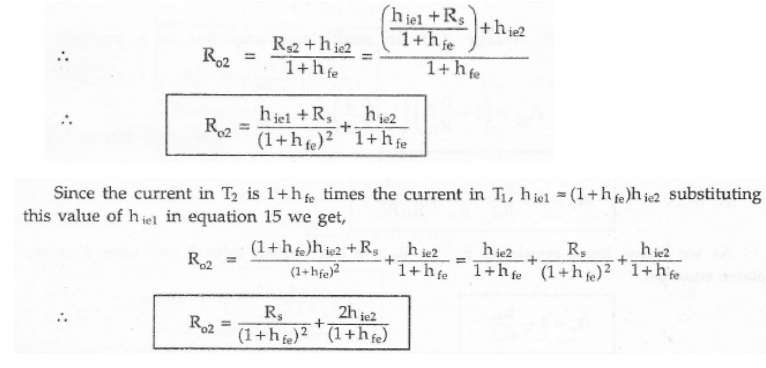
From table, we can say that Darlington connection improves input impedance as well as current gain of the circuit
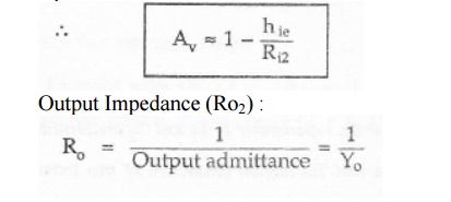
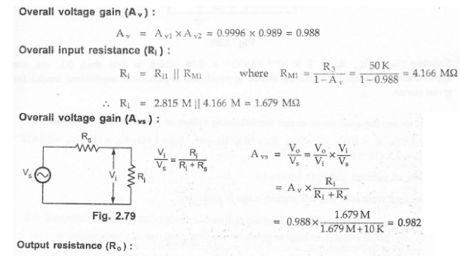
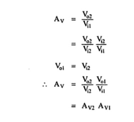
Overall Voltage gain
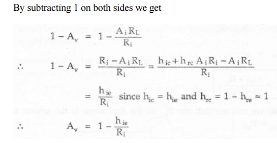
We know that the overall voltage gain in multistage amplifier is a product of individual voltage gain
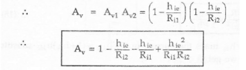
As we know, input resistance Ri1 >> Ri2 we can neglect term 3 and term 4 in the above equation.
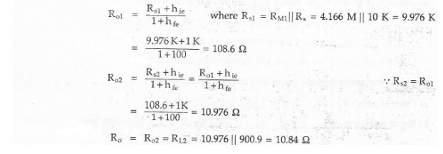
From equation, Yo of the transistor is given as
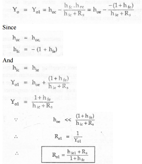
Looking at Figure we can see that the Ri1 of the first stage is the source resistance for second stage, i.e. RS2= RO1
Key Point:
In above analysis we have assumed that the h-parameter of T1 and T2 are identical,
From the above analysis we have seen that Darlington connection of two transistorimproves current gain and input resistance of the circuit.
2. Bootstrap Emitter Follower
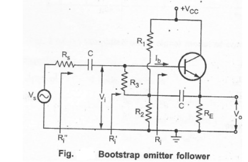
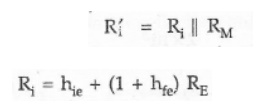
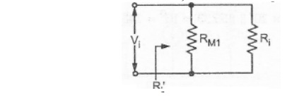
In emitter follower, the input resistance of the amplifier is reduced because of the shunting effect of the biasing resistors. To overcome this problem the emitter follower circuit is modified, as shown in the Figure. Here, two additional components are used, resistance R, and capacitor C .The capacitor, is connected between the emitter and the junction of R1,R2 and R3.
For d.c. signal, capacitor C acts as a open circuit and therefore resistance R1,R2 and R3 provides necessary biasing to keep the transistor in active region.
For ac signal, the capacitor acts as a short circuit. Its value is chosen such that it provides very low reactance nearly short circuit at lowest operating frequency. Hence for ac, the bottom of R3 is effectively connected to the output(the emitter), whereas the top of R3 is at the -input. (the base). In other words, R3 is connected between input node and output node. For such connection effective input resistance is given by Miller's theorem. The two components are
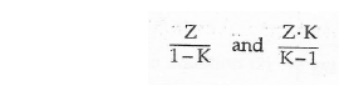
R3 is the impedance between output voltage and input voltage and K is the voltage gain.
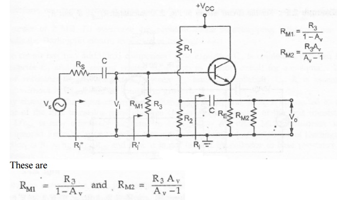
Since, for an emitter follower, Av, approaches unity, then RM2 becomes extremely large.
The above effect, when Av tends to unity is called bootstrapping. The name arises from the fact that, if one end of the resistor R3 changes in voltage, the other end of R3 moves through the same potential difference; it is as if R3 is pulling itself up by its bootstraps.
The effective load on the emitter follower can be given as
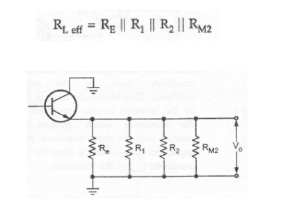
Because of the capacitor, biasing resistances R1 and R2, come on output side shunting effective load resistance. The resistance RM2 is very large and hence it is often neglected.

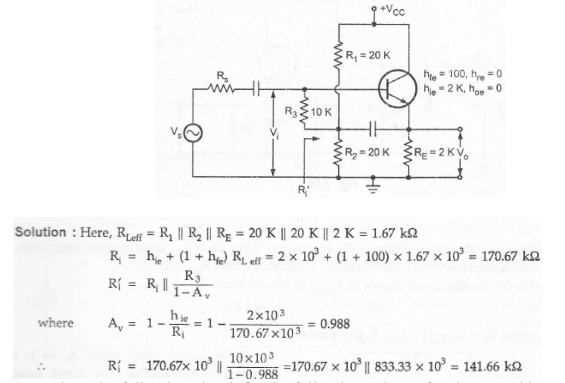
Problem
1. For the circuit shown in Figure calculate RLeff ,Ri, and Ri’
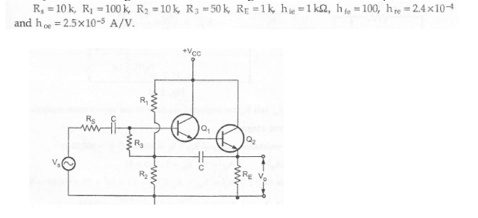
2. Analyze the following circuit for the following values of resistors and h-parameters
Solution
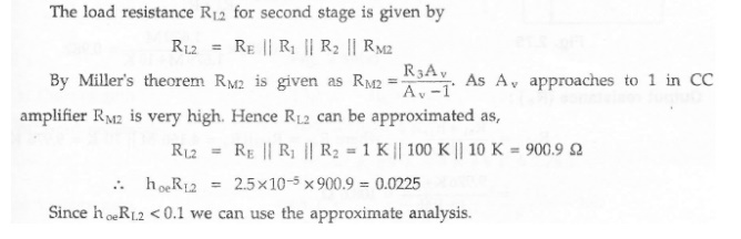
Analysis of second stage
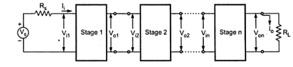
Multistage Amplifiers
In practice, we need amplifier which can amplify a signal from a very weak source such as a microphone, to a level which is suitable for the operation of another transducer
such as loudspeaker . This is achieved by cascading number of amplifier stages, known as multistage amplifier
Need for Cascading
For faithful amplification amplifier should have desired voltage gain, current gain and it should match its input impedance with the source and output impedance with the load. Many times these primary requirements of the amplifier can not be achieved with single stage amplifier, because of the limitation of the transistor/FET parameters. In such situations more than one amplifier stages are cascaded such that input and output stages provide impedance matching requirements with some amplification and remaining middle stages provide most of the amplification.
We can say that,
· When the amplification of a single stage amplifier is not sufficient, or,
· When the input or output impedance is not of the correct magnitude, for a particular application two or more amplifier stages are connected, in cascade. Such amplifier,with two or more stages is also known as multistage amplifier.
Two Stage Cascaded Amplifier
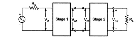
Vi1
is the input of the first stage and Vo2 is the output of second
stage.
So,Vo2/Vi1 is the overall voltage gain of two stage amplifier.
n-Stage Cascaded Amplifier
Voltage gain :
The resultant voltage gain of the multistage amplifier is the product of voltage gains of the various stages.
Av = Avl Av2 ... Avn Gain in Decibels
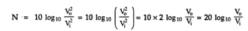
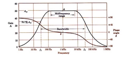
In many situations it is found very convenient to compare two powers on logarithmic scale rather than on a linear scale. The unit of this logarithmic scale is called decibel (abbreviated dB). The number N decibels by which a power P2 exceeds the power P1 is defined by
Decibel, dB denotes power ratio. Negative values of number of dB means that the power P2 is less than the reference power P1 and positive value of number of dB means the power P2 is greater than the reference power P1.
For an amplifier, P1 may represent input power, and P2 may represent output power. Both can be given as
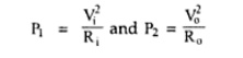
Where Ri and Ro are the input and output impedances of the amplifier respectively.Then,
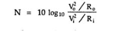
If the input and output impedances of the amplifier are equal i.e. Ri = Ro= R, then
Gain of Multistage Amplifier in dB
The gain of a multistage amplifier can be easily calculated if the gain of the individual stages are known in dB, as shown below
20 log10 Av = 20 log10Avl + 20 log10Av2 +… + 20 log10Avn
Thus, the overall voltage gain in dB of a multistage amplifier is the decibel voltage gains of the individual stages. It can be given as
AvdB = AvldB + Av2dB + ... + AvndB
Advantages of Representation of Gain in Decibels
Logarithmic scale is preferred over linear scale to represent voltage and power gains because of the following reasons :
· In multistage amplifiers, it permits to add individual gains of the stages to calculate overall gain.
· It allows us to denote, both very small as well as very large quantities of linear, scale by considerably small figures.
· For example, voltage gain of 0.0000001 can be represented as -140 dB and voltage gain of 1,00,000 can be represented as 100 dB.
· Many times output of the amplifier is fed to loudspeakers to produce sound which is received by the human ear. It is important to note that the ear responds to the sound intensities on a proportional or logarithmic scale rather than linear scale. Thus use of dB unit is more appropriate for representation of amplifier gains.
Methods of coupling Multistage Amplifiers
In multistage amplifier, the output signal of preceding stage is to be coupled to the input circuit of succeeding stage. For this interstage coupling, different types of coupling
elements can be employed. These are :
1. RC coupling 2 Transformer coupling 3. Direct coupling
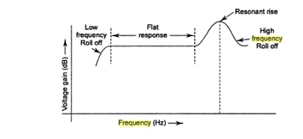
RC coupling
Figure shows RC coupled amplifier using transistors. The output signal of first stage is coupled to the input of the next stage through coupling capacitor and resistive load at the output terminal of first stage
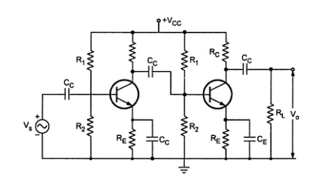
The coupling does not affect the quiescent point of the next stage since the coupling capacitor Cc blocks the d.c. voltage of the first stage from reaching the base of the second stage. The RC network is broadband in nature. Therefore, it gives a wideband frequency response without peak at any frequency and hence used to cover a complete A.F amplifier bands. However its frequency response drops off at very low frequencies due to coupling capacitors and also at high frequencies due to shunt capacitors such as stray capacitance.
Transformer Coupling
Figure shows transformer coupled amplifier using transistors. The output signal of first stage is coupled to the input of the next stage through an impedance matching transformer
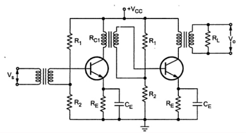
This type of coupling is used to match the impedance between output and input cascaded stage. Usually, it is used to match the larger output resistance of AF power amplifier to a low impedance load like loudspeaker. As we know, transformer blocks d.c, providing d.c. isolation between the two stages. Therefore, transformer coupling does not affect the quiescent point of the next stage. Frequency response of transformer coupled amplifier is poor in comparison with that an RC coupled amplifier. Its leakage inductance and inter winding capacitances does not allow amplifier to amplify the signals of different frequencies equally well. Inter winding capacitance of the transformer coupled may give rise resonance at certain frequency which makes amplifier to give very high gain at that frequency. By putting shunting capacitors across each winding of the transformer, we can get resonance at any desired RF frequency. Such amplifiers are called tuned voltage amplifiers. These provide high gain at the desired of frequency, i.e. they amplify selective frequencies. For this reason, the transformer-coupled amplifiers are used in radio and TV receivers for amplifying RF signals. As d.c. resistance of the transformer winding is very low, almost all d.c. voltage applied by Vcc is available at the collector. Due to the absence of collector resistance it eliminates unnecessary power loss in the resistor.
Direct Coupling
Figure shows direct coupled amplifier using transistors. The output signal of first stage is directly connected to the input of the next stage. This direct coupling allows the quiescent d.c. collector current of first stage to pass through base of the next stage, affecting its biasing conditions
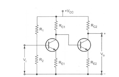
Due to absence of RC components, frequency response is good but at higher frequencies shunting capacitors such as stray capacitances reduce gain of the amplifier.
The transistor parameters such as VBE and β change with temperature causing the collector current and voltage to change. Because of direct coupling these changes appear at the base of next stage, and hence in the output. Such an unwanted change in the output is called drift and it is serious problem in the direct coupled amplifiers.
Related Topics