Chapter: Electronic Circuits : BJT Amplifiers
Important Short Questions and Answers: Electronic Circuits - BJT Amplifiers
BJT AMPLIFIERS
1. What are the advantages of Representation of
Gain in Decibels.
Logarithmic
scale is preferred over linear scale to represent voltage and power gains
because of the following reasons :
• In
multistage amplifiers, it permits to add individual gains of the stages to
calculate overall gain.
• It allows
us to denote, both very small as well as very large quantities of linear, scale
by considerably small figures.
For example,
voltage gain of 0.0000001 can be represented as -140 dB and voltage gain of
1,00,000 can be represented as 100 dB.
• Many
times output of the amplifier is fed to loudspeakers to produce sound which is
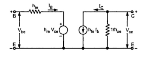
received by the human ear. It is important to note that the ear responds to the
sound intensities on a proportional or logarithmic scale rather than linear
scale. Thus use of dB unit is more appropriate for representation of amplifier
gains.
2. What is the coupling schemes used in multistage
amplifiers?
In
multistage amplifier, the output signal of preceding stage is to be coupled to
the input circuit of succeeding stage. For this interstage coupling, different
types of coupling elements can be employed.
These are
:
1. RC
coupling
2.
Transformer coupling
3. Direct coupling
3.
Define Common Mode Rejection Ratio.
Common
Mode Rejection Ratio is the figure of merit of a differential amplifier to
reject common mode signal and is given by,

4. What does bootstrapping mean? Why bootstrapping
is done in a buffer amplifier?
In the
emitter follower amplifier AV tends to unity. If a resistor is
connected between input and output of the emitter follower, the change in the
voltage at one end of the resistor changes the voltage at the other end of the
resistor by same value. It is as if resistor is pulling itself up by its
bootstraps. Such effect is known as boot
strapping.
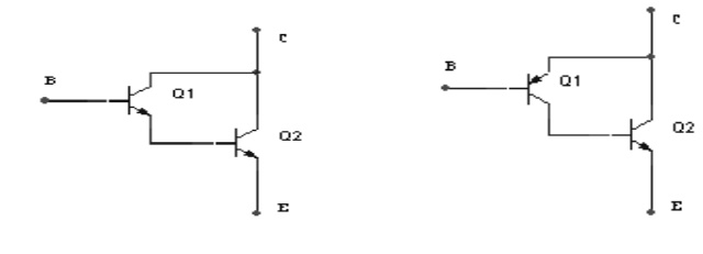
5. Draw the Darlington emitter follower
circuit.

6. How can a DC equivalent circuit of an amplifier
be obtained?
The
analysis of transistor circuits for small signal behaviour can be made by
following simple guidelines. These guidelines are,
• Draw the
actual circuit diagram
• Replace
coupling capacitors and emitter bypass capacitor by short circuit
• Replace
D.C. source by a short circuit
• Mark the
points B, E, C on the circuit diagram and locate these points as the start of
the equivalent circuit
• Replace
the transistor by its h-parameter model
7. State Miller’s Theorem.
It states
that the effect of resistance Z on the input circuit is a ratio of input
voltage to the current which flows from the input to the output.

It states
that the effect of resistance Z on the output circuit is the ratio of output
voltage to the current
which flows from the output to input.

8.
Define i) Differential gain ii) Common mode gain
The gain with which differential
amplifier amplifies the difference between two input signals is called
differential gain of the differential amplifier denoted as A D. The gain
with which it amplifies the common mode signal to produce the output is called
common mode gain of the differential amplifier denoted as A C.
9. What
are practical limitations in selecting very high R E?
1. Large R E needs higher biasing voltage to set the
operating point of the transistors.
2. This increases the overall chip
area. Hence practically R E can not be selected very high.
10.What are the limitations of h
parameters?
The
h parameters has the following limitations,
a. The
accurate calculation of h parameters is difficult.
b. A
transistor behaves as a two port network for small signals only, hence h
parameters can be used to analyze only the small signal amplifiers.
11. What are the advantages of
Darlington amplifier?
A
Darlington transistor connection provides a transistor having a very large
current gain, typically a few thousand. The main features of the Darlington
connection is that the composite transistor acts as a single unit with a
current gain that is the product of current gains of the individual
transistors.
βD=
β1β2
βD
= Darlington connection current gain
β1
and β2 – Current gain of the transistors 1 & 2 in the Darlington pair
12.
Methods of coupling multistage
amplifiers
•
RC
coupling
•
Transformer
coupling
•
Direct
coupling
13.
Features of differential amplifier.
•
High
differential voltage gain
•
Low
common mode gain
•
High
CMRR
•
Two
input terminals
•
High
input impedance
•
Large
bandwidth
•
Low
offset voltages and currents
•
Low
output impedance
14.
List the configuration of
differential amplifiers.
•
Dual
input, balanced output differential amplifier
•
Dual
input, unbalanced output differential amplifier
•
Single
input, balanced output differential amplifier
•
Single
input, unbalanced output differential amplifier
15.
State
Bisection Theorem.
A
particular network which has mirror symmetry with respect to an imaginary line.
If the entire network is denoted as N then it can be divided into two half
networks N/2 about the line of symmetry is called bisection theorem or
Bartlett’s bisection theorem.
16. Methods of improving CMRR
To
improve the CMRR, the common mode gain Ac must be reduced. The common mode gain
Ac approaches zero as RE tends to infinity. This is because RE introduces a
negative feedback in the common mode operation which reduces the common mode
gain Ac. Thus higher the value of RE, lesser is the value of Ac and higher is
the value of CMRR. The differential gain Ad is not dependent on RE
17.
What are
the other methods to improve CMRR without RE?
• Constant
current bias method
• Current
mirror circuit.
18.
List the
advantage of current mirror circuit?
• Provides
very high emitter resistance RE.
• Requires
fewer components than the constant current bias.
• Simple to
design
• Easy to
fabricate.
• With
properly matched transistors, collector current thermal stability is
• achieved.
19.
Draw the
small signal equivalent circuit of CE amplifier.

20. Define Miller effect input capacitance.
For any
inverting amplifier, the input capacitance will be increased by a miller effect
capacitance, sensitive to the gain of the amplifier and the inter electrode
capacitance connected between the input and output terminals of the active
device. CMi = (1- AV) Cf CM0 = Cf Cf = Inter electrode capacitance between
input and output.
Related Topics