Chapter: Electronic Circuits : BJT Amplifiers
Common Base Amplifier Circuit
From given circuit, the signal source is coupled to the emitter of the transistor through C1.
Common Base Amplifier Circuit:
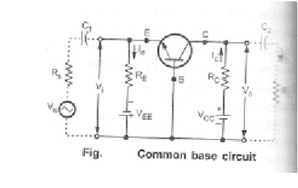
From
above circuit, the signal source is coupled to the emitter of the transistor
through C1. The load resistance RL is coupled to the collector
of the transistor through C2. The positive going pulse of input
source increases the emitter voltage. As base voltage is constant, forward bias
of emitter-base junction reduces. This reduces Ib, Ic and
drop across Rc.
Vo
= VCC - ICRC
Reduction
in IC results in an increase in Vo. Positive going input
produces positive going output and vice versa. So there is no phase shift
between input and output in common base amplifier.
Study Material, Lecturing Notes, Assignment, Reference, Wiki description explanation, brief detail
Electronic Circuits : BJT Amplifiers : Common Base Amplifier Circuit |
Related Topics
Electronic Circuits : BJT Amplifiers