Chapter: Digital Electronics : Minimization Techniques and Logic Gates
TTL Family of ICS
TTL FAMILY OF ICS:
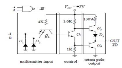
The TTL
NAND gate is broken up into three basic sections: multiemitter input, control
section, and totem-pole output stage. In the multiemitter input section, a
multiemitter bipolar transistor Q1
acts like a two-input ANDgate, while diodesD1
andD2 act as negative clamping diodes
used to protect the inputs from any short-term negative input voltages that
could damage the ransistor. Q2
provides control and current boosting to the totem-pole output stage; when the
output is high (1), Q4 is off (open)
and Q3 is on (short).When the output
is low (0), Q4 is on and Q3 is off. Because one or the other
transistor is always off, the current flow from VCC to ground in that section of the circuit is minimized. The
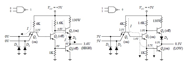
lower figures show both a high and low output state, along with the approximate
voltages present at various locations.
Notice
that the actual output voltages are not exactly 0 or +5V—a result of internal
voltage drops across resistor, transistor, and diode. Instead, the outputs are
around 3.4V for high and 0.3V for low. As a note, to create, say, an
eight-input NAND gate, the multiemitter input transistor would have eight
emitters instead of just two as shown.
A simple
modification to the standard TTL series was made early on by reducing all the
internal resistor values in order to reduce the RC time constants and thus increase the speed (reduce propagation
delays). This improvement to the original TTL series marked the 74H series.
Although the 74H series offered improved speed (about twice as fast) over the
74 series, it had more than double the power consumption. Later, the 74L series
emerged. Unlike the 74H, the 74L took the 74 and increased all internal
resistances. The net effect lead to a reduction in power but increased
propagation delay. A significant improvement in speed within the TTL line
emerged with the development of the 74Sxx
series (Schottky TTL series). The key modifications involved placing Schottky
diodes across the base-to-collector junctions of the transistors. These
Schottky diodes eliminated capacitive effects caused by charge buildup in the transistor’s
base region by passing the charge to the collector region.
Schottky
diodes were the best choice because of their inherent low charge buildup
characteristics. The overall effect was an increase in speed by a factor of 5
and only a doubling in power. Continually over time, by using different
integration techniques and increasing the values of the internal resistors,
more power-efficient series emerged, like the lowpower Schottky 74LS series,
with about one-third the power dissipation of the 74S. After the 74LS, the
advanced-low-power Schottky 74ALS series emerged, which had even better
performance. Another series developed around this time was the 74F series, or
FAST logic, which used a new process of integration called oxide isolation (also used in the ALS series) that led to reduced
propagation delays and decreased the overall size.
Related Topics