Chapter: Digital Electronics : Minimization Techniques and Logic Gates
Important Short Questions and Answers: Minimization Techniques and Logic Gates
MINIMIZATION TECHNIQUES AND
LOGIC GATES
1.
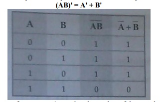
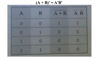
State DemorganŌĆÖs Theorem.
De Morgan suggested two theorems that form
important part of Boolean algebra. They are,
1) The
complement of a product is equal to the sum of the complements.
(AB)' = A' + B'
2) The
complement of a sum term is equal to the product of the complements.
(A + B)' = A'B'
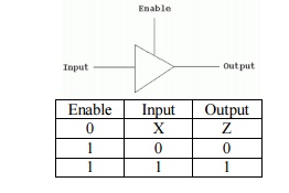
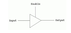
2. Draw an active-high tri-state buffer and write its truth table.
3.
What is a totem pole output?
Totem
pole output is a standard output of a TTL gate. It is specifically designed to
reduce the propagation delay in the circuit and to provide sufficient output
power for high fan-out.
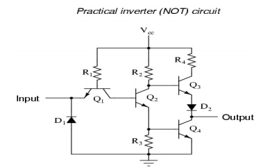
4. Draw the TTL Inverter (NOT) Circuit.
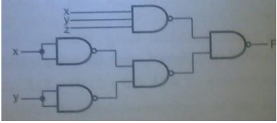
5. Implement using NAND gates only, F=xyz+xŌĆ▓yŌĆ▓
6.
What are DonŌĆÖt care terms?
In some
logic circuits certain input conditions never occur, therefore the
corresponding output never appears. In such cases the output level is not
defined, it can be either high or low. These output levels are indicated by ŌĆśXŌĆÖ
or ŌĆśdŌĆÖ in the truth tables and are called donŌĆÖt care conditions or incompletely
specified functions.
7.
Apply De-MorganŌĆÖs theorem to [(A+B)+C] ŌĆ▓.
Given [(A+B)+C] ŌĆ▓= (A+B) ŌĆ▓.CŌĆ▓
= (AŌĆ▓.BŌĆ▓).CŌĆ▓
[(A+B)+C]
ŌĆ▓ = AŌĆ▓BŌĆ▓CŌĆ▓
8.
Convert 0.35 to equivalent hexadecimal number.
Given
(0.35)10 =0.35 x 16=5.60 =0.60 x 16=9.60 =0.60 x 16=9.60
(0.35)10 =(0.599)16
9.
Convert Y=A+BCŌĆ▓+AB+AŌĆ▓BC
into canonical form.
Given Y=A+BCŌĆ▓+AB+AŌĆ▓BC Y=A(B+BŌĆ▓)(C+CŌĆ▓)+(A+AŌĆ▓)BCŌĆ▓+AB(C+CŌĆ▓)+AŌĆ▓BC Y=ABC+ABCŌĆ▓+ABŌĆ▓C+ABŌĆ▓CŌĆ▓+ABCŌĆ▓+AŌĆ▓BCŌĆ▓+ABC+ABCŌĆ▓+AŌĆ▓BC
Y=ABC+ABCŌĆ▓+ABŌĆ▓C+ABŌĆ▓CŌĆ▓+AŌĆ▓BCŌĆ▓+AŌĆ▓BC
10.
State the advantages of CMOS logic.
┬Ę
Consumes
less power.
┬Ę
Can be
operated at high voltages, resulting in improved noise immunity.
┬Ę
Fan-out
is more.
┬Ę
Better
noise margin.
11.
Define ŌĆśmin termŌĆÖ and ŌĆśmax termŌĆÖ.
(i)
A product
term containing all
the variables of
the function in
either complemented or uncomplemented form is called a min term.
(ii) A
sum term containing all the variables of the function in either complemented or
uncomplemented form is called a max term.
12.
Write a note on tri-state gates.
It is a
digital circuit that exhibits three states. Two of the states are signals
equivalent to logic1 and logic 0. The third state is high impedance state. High
impedance state behaves like a open circuit.
13.
Prove that the logical sum of all min terms of
a Boolean function of 2 variables is 1.
Consider two
variables as A and
B. For two
variables A and B
minterms are:
AŌĆ▓BŌĆ▓,AŌĆ▓B,ABŌĆ▓,AB.
The logical sum of these minterms are given by
F= AŌĆ▓BŌĆ▓+AŌĆ▓B+ABŌĆ▓+AB
= AŌĆ▓(BŌĆ▓+B)+A(BŌĆ▓+B) (BŌĆ▓+B=1)
= AŌĆ▓(1)+A(1) (AŌĆ▓+A=1)
F=1
Hence it
is to be proved.
14.
Show that a positive logic NAND gate is a
negative logic NOR gate.
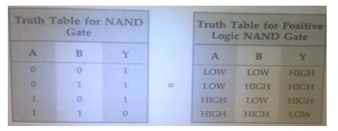
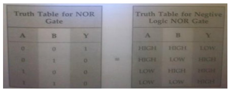
Truth
table for positive logic NAND gate and negative logic NOR gates are same and
hence a positive logic NAND gate is negative logic NOR gate.
15.
What is the significance of high impedance
state in tri-state gates?
┬Ę
High
impedance state of a three-state gate provides a special feature not available
in other gates.
┬Ę
Because
of this features a larger number of three state gate output can be connected
with wires to form a common line without endangering loading effects.
16.
Simplify the following Boolean Expression to a
minimum number of literals.
(BCŌĆ▓+AŌĆ▓D)(ABŌĆ▓+CDŌĆ▓)
F=(BCŌĆ▓+AŌĆ▓D)(ABŌĆ▓+CDŌĆ▓)
=BCŌĆ▓ABŌĆ▓+BCŌĆ▓CDŌĆ▓+AŌĆ▓DABŌĆ▓+AŌĆ▓DCDŌĆ▓
(A.AŌĆ▓=0)
= AB
BŌĆ▓CŌĆ▓+BCCŌĆ▓DŌĆ▓+AAŌĆ▓ BŌĆ▓D+AŌĆ▓CDDŌĆ▓
F=0
17.
Define the term Fan out.
It is
the maximum number of inputs which have same family that the gate can drive
maintaining its output within the specified limits.
18.
Simplify the given Boolean Expression F=xŌĆ▓+xy+xzŌĆ▓+xyŌĆ▓zŌĆ▓.
F=xŌĆ▓+xy+xzŌĆ▓+xyŌĆ▓zŌĆ▓
=
xŌĆ▓+x(y+zŌĆ▓+yŌĆ▓zŌĆ▓) (A+AŌĆ▓B=A+B)
=
xŌĆ▓+y+zŌĆ▓+yŌĆ▓zŌĆ▓
=
xŌĆ▓+y+zŌĆ▓(1+yŌĆ▓) (1+AŌĆ▓=1)
F = xŌĆ▓+y+zŌĆ▓
19.
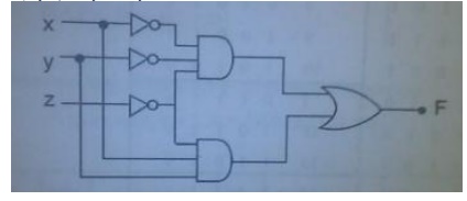
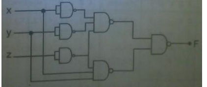
Implement the given function using NAND gates F(x,y,z)= ╬Żm(0,6).
F(x,y,z)=xŌĆ▓yŌĆ▓zŌĆ▓+xyzŌĆ▓
20.
State Distributive Law.
Distributive
law of dot(.) over plus(+) is given by a.(b+c)
= a.b + a.c
Distributive
law of plus(+) over dot(.) is given by a+b.c
= (a+b).(a+c)
21.
What is Prime Implicant?
A prime
implicant is a group of minterms which cannot be combined with any other
minterms or groups.
22.
Simplify the following Boolean expression into
one literal. WŌĆ▓X(ZŌĆ▓+YZ)+X(W+ YŌĆ▓Z)
F= WŌĆ▓X(ZŌĆ▓+YZ)+X(W+ YŌĆ▓Z)
=
WŌĆ▓XZŌĆ▓+WŌĆ▓XYZ+WX+XYŌĆ▓Z
=X(WŌĆ▓ZŌĆ▓+WŌĆ▓YZ+W+YŌĆ▓Z)
=
X(WŌĆ▓ZŌĆ▓+W+Z(YŌĆ▓+WŌĆ▓Y))
=
X(WŌĆ▓ZŌĆ▓+W+Z(YŌĆ▓+ Y )( YŌĆ▓+WŌĆ▓))
=
X(WŌĆ▓ZŌĆ▓+W+Z( YŌĆ▓+WŌĆ▓))
=
X(WŌĆ▓ZŌĆ▓+W+ZYŌĆ▓+WŌĆ▓Z)
=
X(WŌĆ▓(ZŌĆ▓+Z)+W+ZYŌĆ▓)
=
X(WŌĆ▓+W+ZYŌĆ▓)
=
X(1+ZYŌĆ▓)=X.1
F
=X
23.
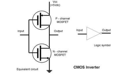
Draw the CMOS inverter circuit.
Related Topics