Chapter: Linear Integrated Circuits : Analog to Digital And Digital to Analog Converters
Successive approximation ADCs
Successive-approximation
ADCs
Successive-approximation
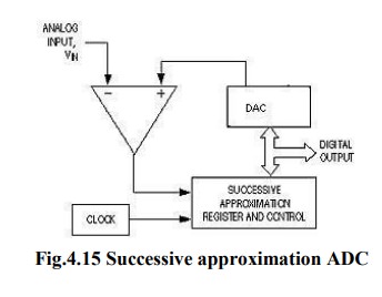
ADC is a conversion technique based on a successive-approximation register
(SAR). This is also called bit-weighing conversion that employs a comparator to
weigh the applied input voltage against the output of an N-bit
digital-to-analog converter (DAC).
The
final result is obtained as a sum of N weighting steps, in which each step is a
single-bit conversion using the DAC output as a reference. SAR converters
sample at rates up to 1Mbps, requires a low supply current, and the cheapest in
terms of production cost.
A
successive-approximation ADC uses a comparator to reject ranges of voltages,
eventually settling on a final voltage range. Successive approximation works by
constantly comparing the input voltage to the output of an internal digital to
analog converter (DAC, fed by the current value of the approximation) until the
best approximation is achieved.
At
each step in this process, a binary value of the approximation is stored in a
successive approximation register (SAR). The SAR uses a reference voltage
(which is the largest signal the ADC is to convert) for comparisons.
For
example if the input voltage is 60 V and the reference voltage is 100 V, in the
1st clock cycle, 60 V is compared to 50 V (the reference, divided by two. This
is the voltage at the output of the internal DAC when the input is a '1'
followed by zeros), and the voltage from the comparator is positive (or '1')
(because 60 V is greater than 50 V). At this point the first binary digit (MSB)
is set to a '1'. In the 2nd clock cycle the input voltage is compared to 75 V
(being halfway between 100 and 50 V: This is the output of the internal DAC
when its input is '11' followed by zeros) because 60 V is less than 75 V, the
comparator output is now negative (or '0'). The second binary digit is
therefore set to a '0'. In the 3rd clock cycle, the input voltage is compared
with 62.5 V (halfway between 50 V and 75 V: This is the output of the internal
DAC when its input is '101' followed by zeros). The output of the comparator is
negative or '0' (because 60 V is less than 62.5 V) so the third binary digit is
set to a 0. The fourth clock cycle similarly results in the fourth digit being
a '1' (60 V is greater than 56.25 V, the DAC output for '1001' followed by
zeros). The result of this would be in the binary form 1001. This is also
called bit-weighting conversion, and
is similar to a binary.
The
analogue value is rounded to the nearest binary value below, meaning this
converter type is mid-rise (see above). Because the approximations are
successive (not simultaneous), the conversion takes one clock-cycle for each
bit of resolution desired.
The
clock frequency must be equal to the sampling frequency multiplied by the
number of bits of resolution desired. For example, to sample audio at 44.1 kHz
with 32 bit resolution, a clock frequency of over 1.4 MHz would be required.
ADCs
of this type have good resolutions and quite wide ranges. They are more complex than some other designs.

Related Topics