Circuit diagram, Advantages | Digital to Analog Converters - Inverted or Current Mode DAC | Linear Integrated Circuits : Analog to Digital And Digital to Analog Converters
Chapter: Linear Integrated Circuits : Analog to Digital And Digital to Analog Converters
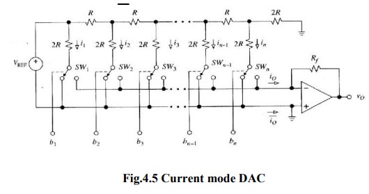
Inverted or Current Mode DAC
Inverted or
Current Mode DAC
Current
mode DACs operates based on the ladder currents. The ladder is formed by resistance
R in the series path and resistance 2R in the shunt path. Thus the current is
divided into i1 , i2, i3 …………in. in each arm. The currents are either diverted
to the ground bus (io) or to the Virtual-ground bus ( io ).
The
currents are given as
i1
= VREF/2R = (VREF/R) 2-1, i2 = (VREF)/2)/2R
= (VREF/R) 2-2 ………in = (VREF/R) 2-n.
And
the relationship between the currents are given as
i2 = i1/2
i3 = i1/4
i4 = i1/8
in = i1/2n-1
Using
the bits to identify the status of the switches, and letting V0 = -Rf io gives
V0
= - (Rf/R) VREF (b12-1 + b22-2+
……….. + bn2-n)
The
two currents io and io are complementary to each other and
the potential of io bus must be
sufficiently close to that of the io
bus. Otherwise, linearity errors will occur. The final op-amp is usedas current
to voltage converter.
Advantages
1.
The
major advantage of current mode D/A converter is that the voltage change across
each switch is minimal. So the charge injection is virtually eliminated and the
switch driver design is made simpler.
2. In Current mode or inverted ladder
type DACs, the stray capacitance do not affect the Speed of response of the
circuit due to constant ladder node voltages. So improved speed performance.
Voltage Mode DAC
This
is the alternative mode of DAC and is called so because the 2R resistance in
the shunt path is switched between two voltages named as VL and VH.
The output of this DAC is obtained from the leftmost ladder node. As the input
is sequenced through all the possible binary state starting from All 0s (0…..0)
to all 1s (1…..1). The voltage of this node changes in steps of 2-n
(VH - VL) from the minimum voltage of Vo = VL
to the maximum of Vo = VH - 2-n (VH - VL).
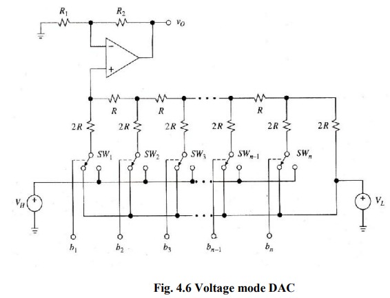
The
diagram also shows a non-inverting amplifier from which the final output is
taken. Due to this buffering with a non- inverting amplifier, a scaling factor
defined by K = 1 + (R2/R1) results.
Advantages
1. The major advantage of this
technique is that it allows us to interpolate between any two voltages, neither
of which need not be a zero.
2. More accurate selection and design
of resistors R and 2R are possible and simple construction.
3. The binary word length can be easily
increased by adding the required number or R-2R sections.
Related Topics