Circuits, Alternative Circuits, Limitations - High Speed Sample and Hold Circuits | Linear Integrated Circuits : Analog to Digital And Digital to Analog Converters
Chapter: Linear Integrated Circuits : Analog to Digital And Digital to Analog Converters
High Speed Sample and Hold Circuits
High Speed
Sample and Hold Circuits
Introduction:
Sample-and-hold
(S/H) is an important analog building block with many applications, including
analog-to-digital converters (ADCs) and switched-capacitor filters. The
function of the S/H circuit is to sample an analog input signal and hold this
value over a certain length of time for subsequent processing.
Taking
advantages of the excellent properties of MOS capacitors and switches,
traditional switched capacitor techniques can be used to realize different S/H
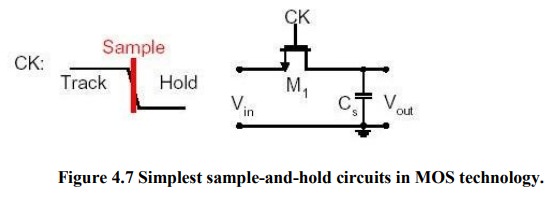
circuits [1]. The simplest S/H circuit in MOS technology is shown in Figure 1,
where Vin is the input signal, M1 is
an MOS transistor operating as the sampling switch, Ch is the hold capacitor,
ck is the clock signal, and Vout is the resulting sample-and-hold output
signal.
As
depicted by Figure 4. , in the simplest sense, a S/H circuit can be achieved
using only one MOS transistor and one capacitor. The operation of this circuit
is very straightforward.
Figure
4, in the simplest sense, a S/H circuit can be achieved using only one MOS
transistor and one capacitor. The operation of this circuit is very
straightforward. Whenever ck is high,
the MOS switch is on, which in turn allows Vout
to track Vin. On the other hand, when
ck is low, the MOS switch is off.
During this time, Ch will keep Vout equal to the value of Vin at the instance when ck goes low.
Unfortunately,
in reality, the performance of this S/H circuit is not as ideal as described
above. The two major types of errors occur. They are charge injection and clock
feed through, that are associated with this S/H implementation. Three new S/H
techniques, all of which try to minimize the errors caused by charge injection
and/or clock feed through.
Alternative CMOS Sample-and-Hold Circuits
Three
alternative CMOS S/H circuits that are developed with the intention to minimize
charge injection and/or clock feed through are
Series Sampling:
The
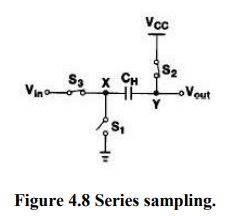
S/H circuit of Figure 4. is classified as parallel sampling because the hold
capacitor is in parallel with the signal. In parallel sampling, the input and
the output are dc-coupled. On the other hand, the S/H circuit shown in Figure 2
is referred to as series sampling because the hold capacitor is in series with
the signal.
When
the circuit is in sample mode, both switches S2 and S3
are on, while S1 is off.
Then,S2 is turned off
first, which means Vout is
equal to VCC (or VDD for most circuits) and
the voltage drop across Ch will be VCC – Vin.
Subsequently, S3 is turned
off and S1 is turned on
simultaneously. By grounding node X, Vout is now equal to VCC –Vin, and the drop from VCC to VCC – Vin is equal to the instantaneous value
of the input.
As
a result, this is actually an inverted S/H circuit, which requires inversion of
the signal at a later stage. Since the hold capacitor is in series with the
signal, series sampling can isolate the common- mode levels of the input and
the output.
This
is one advantage of series sampling over parallel sampling. In addition, unlike
parallel sampling, which suffers from signal-dependent charge injection, series
sampling does not exhibit such behavior because S2 is turned off before S3. Thus, the fact that the gate-to-source voltage, VGS, of S2 is constant means that charge injection coming from S2 is also constant (as opposed to being
signal-dependent), which means this error can be easily eliminated through
differential operation.
Limitations:
On
the other hand, series sampling suffers from the nonlinearity of the parasitic
capacitance at node Y. This parasitic
capacitance introduces distortion to the sample-and hold value, thus mandating that Ch be much larger than the parasitic capacitance. On top of this
disadvantage, the settling time of the S/H circuit during hold mode is longer
for series sampling than for parallel sampling. The reason for this is because
the value of Vout in series sampling
is being reset to VCC (or VDD) for every sample, but this is not
the case for parallel sampling.
Switched Op-Amp Based Sample-and-Hold Circuit:
This
S/H technique takes advantage of the fact that when a MOS transistor is in the
saturation region, the channel is pinched off and disconnected from the drain.
Therefore, if the hold capacitor is connected to the drain of the MOS
transistor, charge injection will only go to the source junction, leaving the
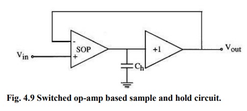
drain unaffected. Based on this concept, a switched op- amp (SOP) based S/H
circuit, as shown in Figure 4.9
During
sample mode, the SOP behaves just like a regular op-amp, in which the value of
the output follows the value of the input. During hold mode, the MOS
transistors at the output node of the SOP are turned off while they are still operating
in saturation, thus preventing any channel charge from flowing into the output
of the SOP. In addition, the SOP is shut off and its output is held at high
impedance, allowing the charge on Ch
to be preserved throughout the hold mode. On the other hand, the output buffer
of this S/H circuit is always operational during sample and hold mode and is
always providing the voltage on Ch to
the output of the S/H circuit.
S/H
circuits that operate in closed loop configuration can achieve high resolution,
but their requirements for high gain circuit block, such as an op-amp, limits
the speed of the circuits. As a result, better and faster S/H circuits must be
developed.
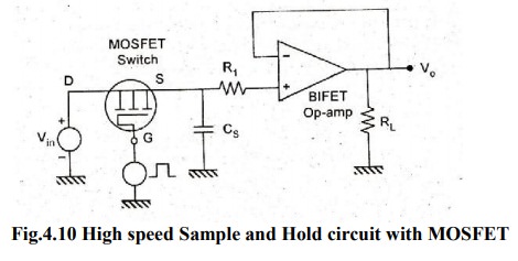
The
above figure shows a sample and holds circuit with MOSFET as Switch acting as a
sampling device and also consists of a holding capacitor Cs to store the sample
values until the next sample comes in. This is a high speed circuit as it is
apparent that CMOS switch has a very negligible propagation delay.
Three
S/H circuits to reduce error:
o
series
sampling,
o
SOP
based S/H circuit,
o bottom
plate S/H circuit with bootstrapped switch
Related Topics