Analog to Digital Converters - A to D Converter- Specifications | Linear Integrated Circuits : Analog to Digital And Digital to Analog Converters
Chapter: Linear Integrated Circuits : Analog to Digital And Digital to Analog Converters
A to D Converter- Specifications
A to D
Converter- Specifications
Like
DAC, ADCs are also having many important specifications. Some of them are
Resolution, Quantization error, Conversion time, Analog error, Linearity error,
DNL error, INL error & Input voltage range.
Resolution:
The
resolution refers to the finest minimum change in the signal which is accepted
for conversion, and it is decided with respect to number of bits. It is given
as 1/2n, where ‘n’ is the number of bits in the digital output word.
As it is clear, that the resolution can be improved by increasing the number of
bits or the number of bits representing the given analog input voltage.
Resolution
can also be defined as the ratio of change in the value of input voltage Vi,
needed to change the digital output by 1 LSB. It is given as
Resolution
= ViFS / (2n – 1)
Where
‘ViFS’ is the full-scale input voltage.
‘n’
is the number of output bits.
Quantization error:
If
the binary output bit combination is such that for all the values of input
voltage Vi between any two voltage levels, there is a unavoidable uncertainty
about the exact value of Vi when the output is a particular binary combination.
This uncertainty is termed as quantization error. Its value is ± (1/2) LSB. And
it is given as,
QE
= ViFS / 2(2n – 1)
Where
‘ViFS’ is the full-scale input voltage
‘n’
is the number of output bits.
Maximum
the number of bits selected, finer the resolution and smaller the quantization
error.
Conversion Time:
It
is defined as the total time required for an A/D converter to convert an analog
signal to digital output. It depends on the conversion technique and
propagation delay of the circuit components.
Analog error:
An
error occurring due to the variations in DC switching point of the comparator,
resistors, reference voltage source, ripples and noises introduced by the
circuit components is termed as Analog error.
Linearity Error:
It
is defined as the measure of variation in voltage step size. It indicates the
difference between the transitions for a minimum step of input voltage change.
This is normally specified as fraction of LSB.
Differential Non-Linearity(DNL) Error:
The
analog input levels that trigger any two successive output codes should differ
by 1 LSB. Any deviation from this 1 LSB value is called as DNL error.
Integral Non-Linearity (INL) Error:
The
deviation of characteristics of an ADC due to missing codes causes INL error.
The maximum deviation of the code from its ideal value after nulling the offset
and gain errors is called as Integral Non-Linearity Error.
Input Voltage Range:
It
is the range of voltage that an A/D converter can accept as its input without
causing any overflow in its digital output.
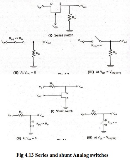
Analog Switches
There
were two types of analog switches. Series and Shunt switch. The Switch
operation is shown for both the cases VGS=0 VGS= VGs (off)
Related Topics