Chapter: Physics : Semiconducting Materials
Semiconducting Materials
Semiconducting Materials
1 Introduction
1.1 Properties of semiconductor
2 Classification of Semiconductors
2.1 Intrinsic semiconductors
2.2 Compound Semiconductors
2.3 Difference between N-type and P-type semiconductor
2.4 Difference between Elemental and Compound Semiconductors
3 Classification of Conductors, Insulators and Semiconductors Based on Band Theory
3.1 Conductors
3.2 Insulators
3.3 Semiconductors
3.4 Mobility and Conductivity in Semiconductors
4 Carrier Concentration in Intrinsic Semi-conductors
4.1 Density of electrons in conduction band
4.2 Density of Holes in Valence band
4.3 Intrinsic Carrier Concentration
5 Fermi level and variation of fermi level with temperature in an intrinsic semiconductor
6 Density of Electrons and Holes In Terms of Eg
7 Variation of Fermi level in Intrinsic semiconductor
8 Electrical Conductivity in Intrinsic Semi-conductor
9 Determination of Band Gap Energy of a Semiconductor
10 Extrinsic Semiconductor
10.1 N-type Semiconductor (Donor impurity)
10.2 P – type Semiconductor (Acceptor Impurities)
11 Charge Densities in a Semiconductor
12 Carrier Concentration in P-type Semi-conductor
12.1 Expression for the density of holes in valence band in termsof NA
13 Carrier Concentration in N-type Semi Conductor
13.1 Expression for the density of electrons in conduction band in terms of ND
14 Variation of Fermi Level with Temperature and Concentration of Impurities in P-type Semiconductor
15 Variation of Fermi Level with Temperature and Concentration of Impurities in N-type Semiconductor
16 Hall Effect
16.1 Hall Effect
16.2 Hall Effect in n –type Semiconductor
16.3 Hall Effect in p-type Semiconductor
16.4 Hall Coefficient Interms of Hall Voltage
16.5 Experimental Determination of Hall Effect
16.6 Application of Hall Effect
1 INTRODUCTION
A semiconductor has electrical conductivity between that of a conductor and an insulator. Semiconductors differ from metals in their characteristic property of decreasing electrical resistivity with increasing temperature. Semiconductors can also display properties of passing current more easily in one direction than the other, and sensitivity to light.
Because the conductive properties of a semiconductor can be modified by controlled addition of impurities or by the application of electrical fields or light, semiconductors are very useful devices for amplification of signals, switching, and energy conversion. The comprehensive theory of semiconductors relies on the principles of quantum physics to explain the motions of electrons through a lattice of atoms.
Current conduction in a semiconductor occurs via free electrons and holes, collectively known as charge carriers. Adding a small amount of impurity atoms greatly increases the number of charge carriers within it. When a doped semiconductor contains excess holes it is called “p-type,” and when it contains excess free electrons it is known as “n-type”.
The semiconductor material used in devices is doped under highly controlled conditions to precisely control the location and concentration of p- and n-type dopants. A single semiconductor crystal can have multiple p and n type regions; the p-n junctions between these regions have many useful electronic properties.
Semiconductors are the foundation of modern electronics, including radio, computers, and telephones. Semiconductor-based electronic components include transistors, solar cells, many kinds of diodes including the light-emitting diode (LED), the silicon controlled rectifier, photo-diodes, digital analog integrated circuits. Increasing understanding of semiconductor materials and fabrication processes has made possible continuing increases in the complexity and speed of semiconductor devices, an effect known as Moore’s Law.
Properties of semiconductor
The resistivity of semiconductors lies between a conductor and an Insulator. (It various from 10–4 to 0.5 m).
At 0 K it behave as insulator.
They have negative temperature Coefficient of resistance. ( when the temperature is increased large number of charge carriers are produced due to breaking of covalent bonds and hence these electrons move freely and gives rise to conductivity)
In semiconductors, both electrons and holes are charge carriers.
If we increase the temperature of semiconductor, its electrical conductivity also increases.
They have an empty conduction band and almost filled valence band 0 K.
They are formed by a covalent bonds.
They have small energy gap (or) band gap.
2 CLASSIFICATION OF SEMICONDUCTORS
Based on the purity, semiconductor is classified into two types.
Intrinsic semiconductors or Elemental semiconductors
Extrinsic semiconductors or Compound semiconductors
2.1 Intrinsic semiconductors
A pure semiconductor without any impurities is known as an intrinsic semiconductor.
Example: Ge, Si (In the form of pure)
These are made from single element. They also known as indirect band gap semiconductors. In which the recombination of free electron from the conduction band with the hole in the valence band takes place via traps. During recombination phonons [lattice vibrations] are produced and they heat the crystal lattice (position of the atom). These are the IV group element in the periodic table.
2.2 Compound Semiconductors
The Compound Semiconductor is a semiconductor compound composed of elements from two or more different groups of the periodic table. They also known as direct band gap semiconductors.
i.e., III – V group, II – VI group and IV – VI group.
Here the recombination electron and hole takes place directly, during recombination photons are emitted.
Example : GaAs, GaP,
Based on the type of impurity they are classified into
i) N-type semiconductor
P-type semiconductor
2.3 Difference between N-type and P-type semiconductor
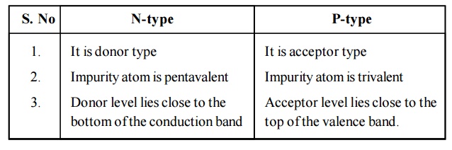
N-type
1. It is donor type
2. Impurity atom is pentavalent
3. Donor level lies close to the bottom of the conduction band
P-type
1. It is acceptor type
2. Impurity atom is trivalent
3. Acceptor level lies close to the top of the valence band.
2.4 Difference between Elemental and Compound Semiconductors
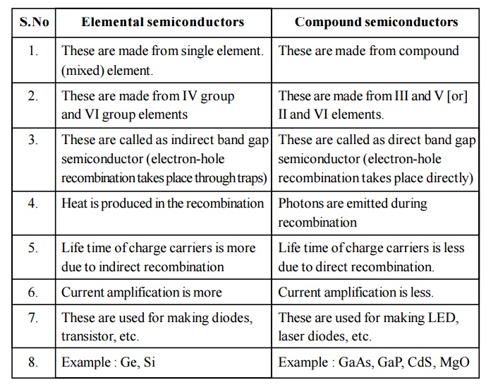
Elemental semiconductors
These are made from single element. (mixed) element.
These are made from IV group and VI group elements
These are called as indirect band gap semiconductor (electron-hole recombination takes place through traps)
Heat is produced in the recombination
Life time of charge carriers is more due to indirect recombination
Current amplification is more
These are used for making diodes, transistor, etc.
Example : Ge, Si
Compound semiconductors
These are made from compound
These are made from III and V [or] II and VI elements.
These are called as direct band gap semiconductor (electron-hole recombination takes place directly)
Photons are emitted during recombination
Life time of charge carriers is less due to direct recombination.
Current amplification is less.
These are used for making LED, laser diodes, etc.
Example : GaAs, GaP, CdS, MgO
3 CLASSIFICATION OF CONDUCTORS, INSULATORS AND SEMICONDUCTORS BASED ON BAND THEORY
The electrical conduction properties of different elements and compounds can be explained in terms of the electrons having energies in the valence and conduction bands. The electrons lying in the lower energy bands, which are normally filled, play no part in the conduction process.
3.1 Conductors
Conductors are those materials in which plenty of free electrons are available for electric conduction.
In terms of energy bands, it means that electrical conductors are those which have overlapping valence and conduction bands as shown in Figure. In fact, there is no physical distinction between the two bands, hence, the availability of a large number of conduction electrons.
Hence the free electrons can easily move from the valence band to conduction band, and are available for electrical conduction under the action of an electric field.
Another point worth noting is that in the absence of forbidden energy band in good conductors, there is no structure to establish holes. The total current in such conductors is simply a flow of electrons. It is exactly for this reason that the existence of holes was not discovered until semiconductors were studied thoroughly.
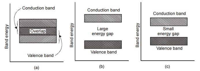
Fig.2.1 Energy band gap (a) conductor (b) insulator and (c) semiconductor
3.2 Insulators
Stated simply, insulators are those materials in which valence electrons are tightly bonded to their parent atoms, thus requiring very large electric field to remove them from the attraction of the nuclei.
Have a filled valence band
Have an empty conduction band and
Have a large energy gap (the order of > 3 eV) between them.
This is shown in Fig. 2.1(b). For conduction process, electrons must be given sufficient energy to jump from the valence band to the conduction band. Increase in temperature enables some electrons to go to the conduction band which infact accounts for the negative resistance – temperature coefficient of insulators. Only at very high temperature, the thermal energy will be sufficient to raise the electrons from valence band to conduction band. Therefore at high temperatures even insulators can conduct electric current.
3.3 Semiconductors
A semiconductor material is one whose electrical properties lie in between those of insulators and good conductors. (Example: Ge, Si).
In terms of energy band, semiconductors can be defined as those materials which have almost an empty conduction band and almost filled valence band with a very narrow energy gap (of the order of 1 eV) separating the two as shown in Figure.
In semiconductors, there is a small energy gap. Hence, the electrons require small energy to jump from valence band to conduction band. This energy may be in the form of heat or light. Even at room temperature, the thermal energy is sufficient to transfer electrons from valence band to conduction band. But when the semiconductor is at zero Kelvin, the thermal energy is not sufficient to transfer the electrons from the valence band to conduction band.
Semiconductors at 0K behave like insulators. In semiconductors the resistance decreases with increase in temperature.
The resistivity of the above three classes of materials as follows
Conductors = 10–8 to 10–6 ohm m
Insulators = 1010 to 1016 ohm m
Semiconductors = 10–4 to 0.5 ohm m
3.4 Mobility and Conductivity in Semiconductors
When an electric field (E) is applied to a semiconductor, the free electrons and holes are drifted in opposite direction of the electric field, due to this a current is produced called drift velocity (Vd)
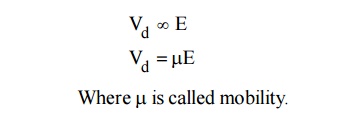
Mobility is defined as the ratio of drift velocity to the applied electric field.
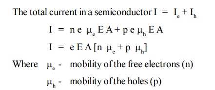
In the case of intrinsic semiconductor, number of free electrons [n] in the conduction band is equal to the number of holes [p] in the valence band.
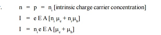
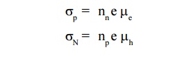
The electrical conductivity of the intrinsic semiconductor is due to drifting action of electrons and holes is given by,

The electrical conductivity of the extrinsic semiconductor is
4 CARRIER CONCENTRATION IN INTRINSIC SEMI-CONDUCTORS
In a semiconductor both electrons and holes are charge carriers (know as carrier concentration). A semiconductor in which holes and electrons are created by thermal excitation across the energy gap is called an intrinsic semiconductor.
In an intrinsic semiconductor the number of holes is equal to the number of free electrons.
At T = 0K, valence band is completely filled and conduction band is completely empty. Thus the intrinsic semiconductor behaves as a perfect insulator.
At T > 0K, the electron from the valence band shifted to conduction band across the band gap.
Thus there are number of free electrons and holes in intrinsic semiconductor. Fermi level lies in midway between conduction band and valance band in intrinsic semiconductors.
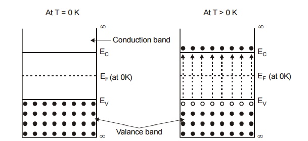
Fig. 2.2 Energy Band Diagram in an Intrinsic Semiconductor
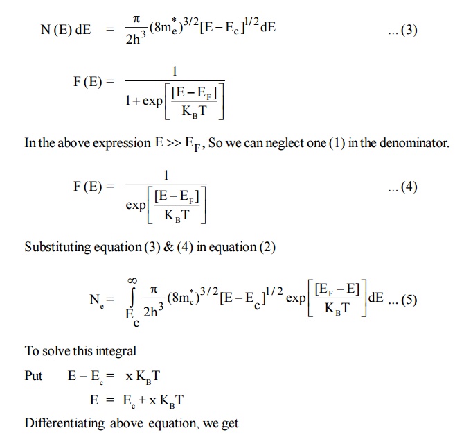
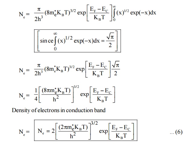
4.1 Density of electrons in conduction band
Let dN be the number of electrons in the energy interval E and E + dE in the conduction band.
dN = N(E) dE F(E) ... (1)
Where N (E) dE is the density of states in the energy interval E and E + dE and F (E) is the probability that a state of energy E is occupied.
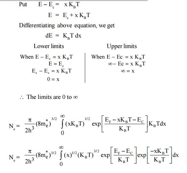
The number of electrons in conduction band can be calculated by integrating the equation(1) from energy Ec (ie., energy from the bottom of the conduction Ec to the top of conduction band ininity)
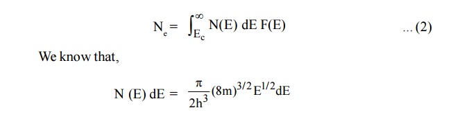
Since, the semiconductor is a crystal, the electron motion is considered in the periodic potential. So, the mass ‘m’ is replaced as effective mass m *e and the kinetic energy of the electron, E = E – Ec
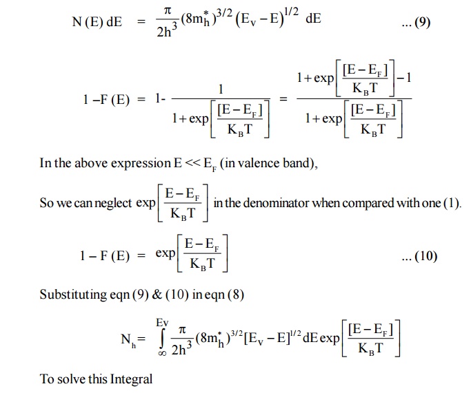
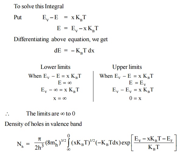
4.2 Density of Holes in Valence band
Let dP be the number of holes in the energy interval E and E + dE in the valence band.

(1– F (E) is the remaining probability after finding the density of electrons) The total number of holes within limits to Ev is
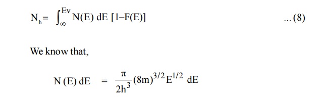
Since, the semiconductor is a crystal, the electron motion is considered in the periodic potential. So, the mass m is replaced as effective mass mh and the kinetic energy of the electron, E = Ev – E.
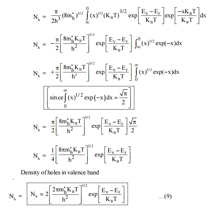
4.3 Intrinsic Carrier Concentration
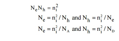
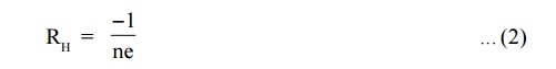
In intrinsic semiconductors Ne = Nh = ni is called intrinsic carrier concentration.
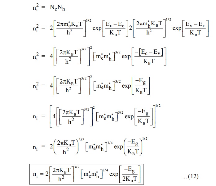
The equation (12) is called as intrinsic carrier concentration.
Where Eg = Ec-Ev is the energy gap between conduction band and valence
band.
Therefore for intrinsic semiconductor even if impurity is added to increase Ne there will be decrease in Nh and hence the product Ne Nh will remain constant. This is called Law of mass action.
5 FERMI LEVEL AND VARIATION OF FERMI LEVEL WITH TEMPERATURE IN AN INTRINSIC SEMICONDUCTOR
Derivation of Fermi Level
In an intrinsic semiconductor,
i.e., Density of electrons ( Ne ) = Density of holes ( Nh )
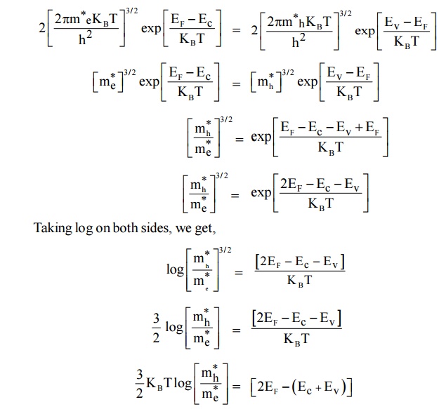
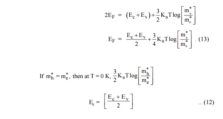
Therefore, the Fermi level lies in the midway between Conduction level Ec and Valence level Ev at T = 0K.
But in general mh = me so the Fermi level is a function of temperature and is raised slightly with temperature.
6 DENSITY OF ELECTRONS AND HOLES IN TERMS OF Eg
In terms of energy gap ( Eg ). Where Eg Ec Ev we can get the expressions of Ne and Nh by substituting the value of EF in terms of Ec and Ev
Substituting equation (13) in equation (6) we get,
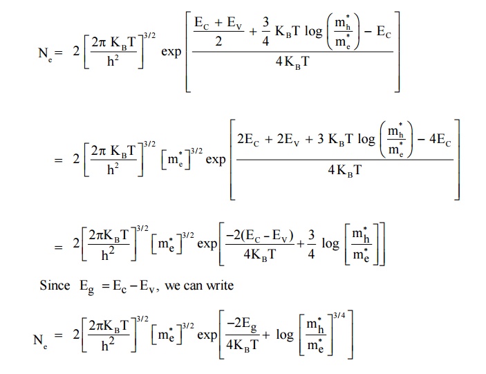
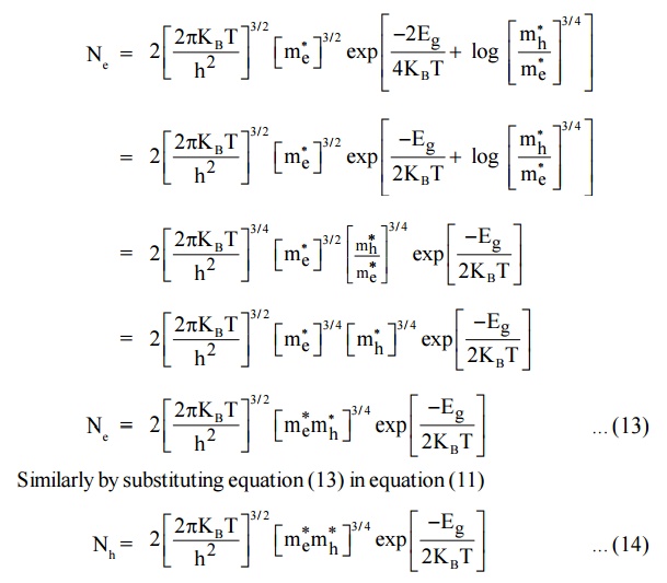
Thus, it is found that Ne = Nh = ni where ni is a intrinsic carrier concertration.
7 VARIATION OF FERMI LEVEL IN INTRINSIC SEMICONDUCTOR
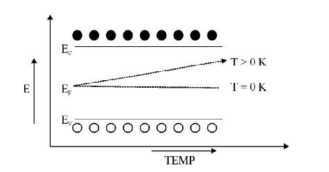
Fig. 2.3 Variation of Fermi level in Intrinsic semiconductor
At T = 0 K, the Fermi level lies exactly in midway between conduction band and Valence band.
At T > 0 K, the Fermi level rises slightly upward since m h > m e .
8 ELECTRICAL CONDUCTIVITY IN INTRINSIC SEMI-CONDUCTOR
Expression for electrical conductivity in intrinsic semiconductor
The general expression for the electrical conductivity,

The intrinsic electrical conductivity,
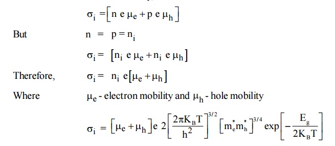
The electrical conductivity depends on the negative exponential of band gap Eg between the valance band and conduction band and also for the mobilities of both holes and electrons. The mobilities in a pure semiconductor are determined by the interaction of electron with lattice waves or phonons.
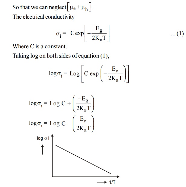
Fig. 2.4 Variation of Electrical with temperature in intrinsic semiconductor
A graph is drawn between 1/T and Log i from the graph it is noted that this electrical conductivity increases with temperature.
9 DETERMINATION OF BAND GAP ENERGY OF A SEMICONDUCTOR
We know that the electrical conductivity,
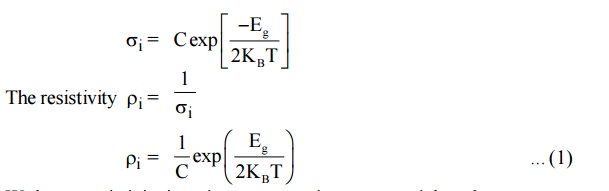
We know resistivity is resistance per unit area per unit length
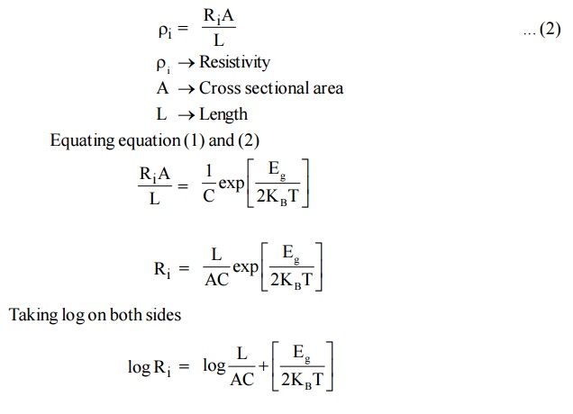
The above equation gives us a method of determining the energy gap of an intrinsic material. If we find the resistance of the intrinsic semiconductor using post office box or carry Foster’s bridge at various temperatures, we can plot a graph between 1/T and log Ri
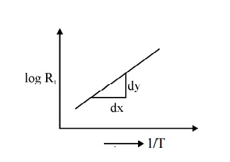
Fig. 2.5 Variation of resistance with temperature in intrinsic semiconductor
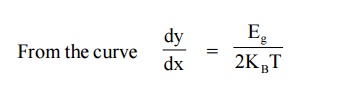
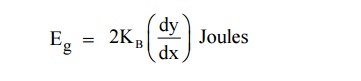
Therefore by finding the slope of line we can calculate the energy band gap with the following expression.
10 EXTRINSIC SEMICONDUCTOR
A semiconductor in which the impurity atoms are added by doping process is called Extrinsic semiconductor. The addition of impurities increases the carrier concentration and conductivity. There are two types of impurities.
Donor impurity which leads to N-type semiconductor.
Acceptor impurity which leads to P-type semiconductor.
10.1 N-type Semiconductor (Donor impurity)
Donor impurity means it donates the electron to the semiconductor materials.
Pentavalent atoms (five valence electrons in their outer most orbit) are called as donor impurities. Example : Phosphorous, Arsenic and Antimony.
When a pentavalent atom is added with tetravalent atoms (Ge and Si), the covalent bond is formed and one element is left free. Thus one impurity atom is surrounded by four Ge or Si atoms.
The remaining electron is loosely bound to the parent impurity atom is detached from the impurity atom by supplying ionization energy.
Each impurity atom donates one free electron. Thus this type of semiconductor is called as N-type semiconductor.
The donor atoms form the new energy level called donor energy level ( ED ) very near and below the conduction band.
At room temperature, almost all the excess electrons donated by the donor atoms are raised to the conduction band as majority charge carriers (free electrons) in N-type semiconductor.
Fig. 2.6 N type semiconductor
10.2 P – type Semiconductor (Acceptor Impurities)
Acceptor impurity means it ready to accept an electron to form the covalent bond in semiconductor materials.
Trivalent atoms (three valence electrons in their outer most orbits) are called as acceptor impurities. Example: Aluminum, Gallium, Boron and Indium.
When a trivalent atom is added with tetravalent atoms (Ge or Si), the covalent bond is formed and there is one vacancy (hole) for one electron in one of the covalent bonds, thereby one impurity atom is surrounded by four Ge or Si atoms.
Thus each impurity atom hole is ready to accept an electron. Thus this type of semiconductor is called P-type semiconductor.
The Acceptor atoms form the new energy level called acceptor energy level (EA) very near and above the valence band.
When a small amount of energy is applied, the electrons from valence band are moved to the acceptor level and creating holes in the valence band.
These valence band holes are the majority charge carriers in the P-type semiconductor material.
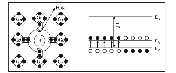
Fig. 2.7 P type semiconductor
11 CHARGE DENSITIES IN A SEMICONDUCTOR
In intrinsic semiconductor, the electron density is equal to hole density.
In Extrinsic semiconductor the electron and hole densities are related by

The law of charge neutrality also relate the densities of free electron and holes in an Extrinsic semiconductor.
The law of charge neutrality states that the total positive charge density is equal to the total negative charge density.
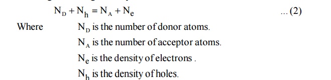
Case 1:
In N-type semiconductors, there is no acceptor doping atoms. i.e., NA =0 and also the majority carriers are electrons. The number of electrons is greater than the number of holes.

equation (2) becomes ND = Ne
Thus in N-type material, the free electron concentration equals to the density of donor atoms.
Case 2:
In the P-type semiconductor, there is no donor doping atoms. i.e., ND 0 and also the majority carriers are holes. The number of holes is greater than the number of electrons.

Thus P-type material, the hole concentration equals to the density of acceptor atoms. According to the law of mass action.
12 CARRIER CONCENTRATION IN P-TYPE SEMI- CONDUCTOR
P-Type Semiconductor : If trivalent (Aluminum, Gallium, Indium) impurities are doped with pure semiconducting material the holes are produced, this is called P - type semiconductor.
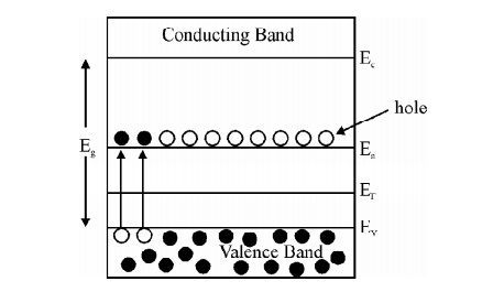
Fig. 2.8 Energy level diagram for P-type Semiconductor
We know that,
Density of holes in the valence band in an intrinsic semiconductors is
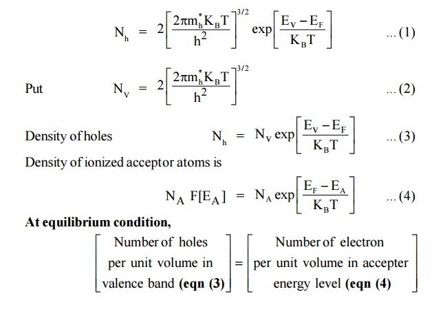
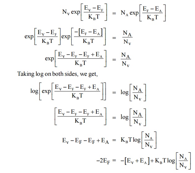

At 0 K fermi level in p type semiconductor lies exactly at the middle of the acceptor level and the top of the valance band.
Expression for the density of holes in valence band in termsof NA
As the temperature is increased more and more the acceptor atoms are ionized. Further increase in temperature results in generation of electron hole pairs due to breaking of covalent bonds and materials tends to behave in a intrinsic manner. The fermi level gradully moves towards the intrinsic fermi level.
We know density of holes in valence band
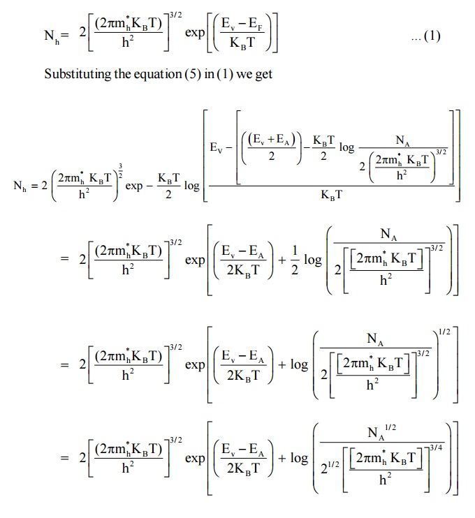
Here EA – EV = E is known as ionisation energy of acceptors i.e. E represents the energy required for an electron to move from valance band (EV) to acceptor energy level (EA)
13 CARRIER CONCENTRATION IN N-TYPE SEMI CONDUCTOR
If pentavalent (Phosphorous, Arsenic, Antimony) impurities are doped with pure semiconducting material the free electrons are produced, this is called N-type semiconductor.
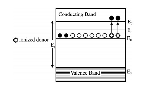
Fig. 2.9 Energy level diagram for N-type Semiconductor
We know that,
Density of electrons in conduction band in an intrinsic semiconductor is
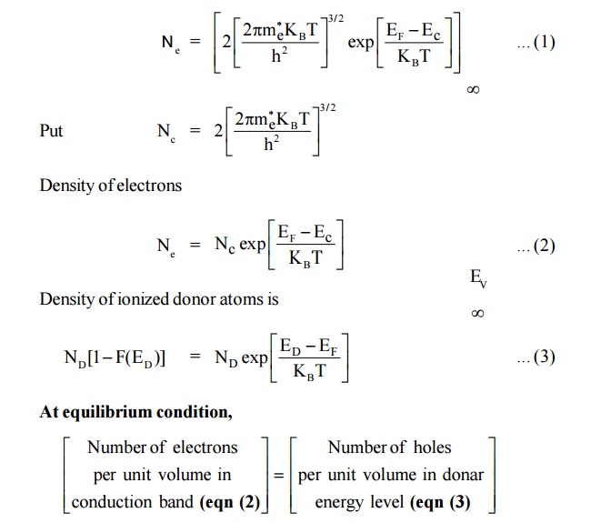
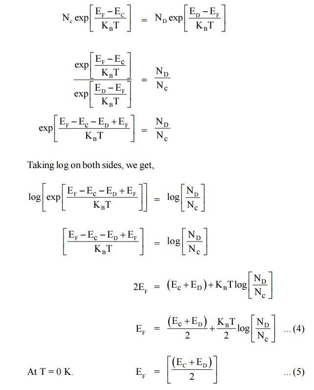
At T = 0 K. Thus, the Fermi level in N-type semiconductor lies exactly in middle of the conduction level (EC) and donor level (ED).
This equation shows that the electron concentration in the conduction band is proportional to the square root of the donor concentration.
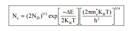
13.1 Expression for the density of electrons in conduction band in terms of ND
As the temperature is increased more and more the donor atoms are ionized and the fermi level drops. For a particular temperature all donor atoms are ionized, further increase in temperature results in generation of electron hole pairs due to breaking of covalent bonds and materials tends to behave in a intrinsic manner.
We know density of electrons in conduction band

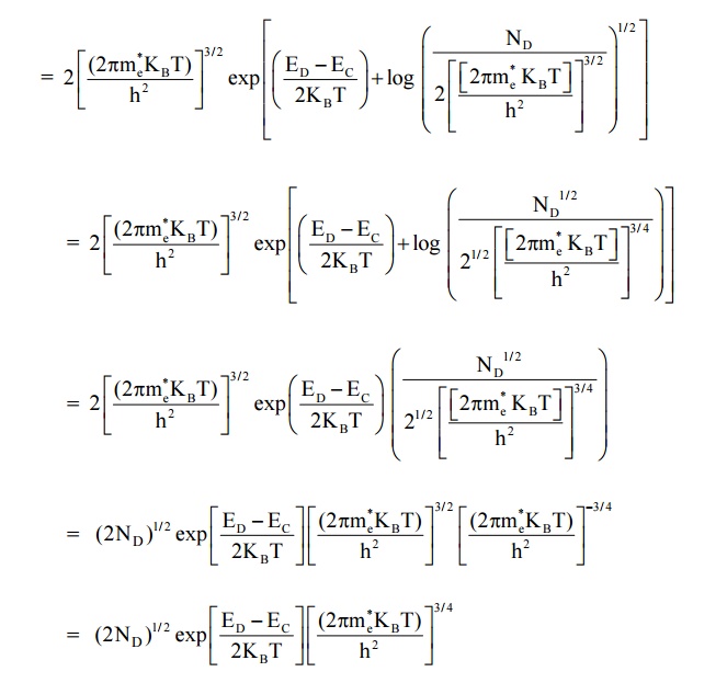
Here EC – ED = E is known as ionisation energy of donars i.e. E represents the amount of energy required to transfer on an electron to from donor envergy level (ED) to conduction band (EC)
14 VARIATION OF FERMI LEVEL WITH TEMPERATURE AND CONCENTRATION OF IMPURITIES IN P-TYPE SEMICONDUCTOR
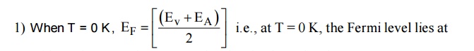
mid way between the acceptor level and valence level.
When temperature increases, some of the electrons from valence band will go to acceptor energy level [EA]. Therefore the Fermi level shifts upward. At high temperature 500 K, the Fermi level reaches intrinsic levelEi .
If the impurity atoms are increased from 1021 atoms /m3 to 1024 atoms / m3 the hole concentration increases and hence the Fermi level decrease.
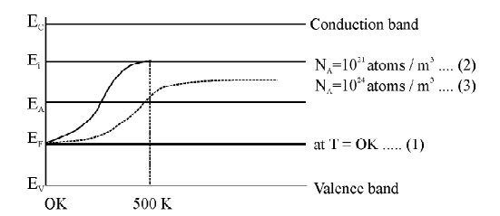
Fig. 2.10 variation of Fermi level with Temperature and Concentration of Impurities in P-type Semiconductor.
15 VARIATION OF FERMI LEVEL WITH TEMPERATURE AND CONCENTRATION OF IMPURITIES IN N-TYPE SEMICONDUCTOR
mid way between the Donar level and valence level.
When temperature increases, some of the electrons moves from valence band to Donar energy level [ED]. Therefore the Fermi level shifts upward. At high temperature 500 K, the Fermi level reaches intrinsic levelED .
If the impurity atoms are increased from 1021 atoms /m3 to 1024 atoms / m3, the electron concentration increases and hence the Fermi level decrease.
Fig. 2.11 variation of Fermi level with Temperature and Concentration of Impurities in N-type Semiconductor.
16 HALL EFFECT
Measurement of conductivity will not determine whether the conduction is due to electron or holes and therefore will not distinguish between p-type and n-type semiconductor.
Therefore Hall Effect is used to distinguish between the two types of charge carriers and their carrier densities and is used to determine the mobility of charge carriers.
16.1 Hall Effect
When conductor (metal or semiconductor) carrying a current is placed in a transverse magnetic field, an electric field is produced inside the conductor in a direction normal to both the current and the magnetic field. This phenomenon is known as “Hall effect” and the generated voltage is called “Hall voltage”.

16.2 Hall Effect in n –type Semiconductor
Let us consider an n-type material to which the current is allowed to pass along x-direction from left to right (electrons move from right to left) and the magnetic field is applied in z-directions, as a result Hall voltage is produced in y direction.
Since the direction of current is from left to right the electrons moves from right to left in x-direction as shown in Figure.
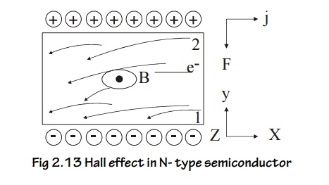
Fig 2.13 Hall effect in N- type semiconductor
Now due to the magnetic field applied the electrons move towards downward direction with the velocity ‘v’ and cause the negative charge to accumulate at face (1) of the material as shown Figure.
Therefore a potential difference is established between face (2) and face (1) of the specimen which gives rise to field EH in the negative y direction.
The negative sign indicates that the field is developed in the negative ‘y’ direction.
16.3 Hall Effect in p-type Semiconductor
Let us consider a p-type material for which the current is passed along x-direction from left to right and magnetic field is applied along z-direction as shown in Figure Since the direction of current is from left to right, the holes will also move in the same direction.
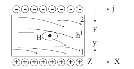
Fig 2.14 Hall effect in P- type semiconductor
Now due to the magnetic field applied, the holes move towards the downward direction with velocity ‘v’ and accumulate at the face (1) as shown in Figure.
A potential difference is established between face (1) and (2) in the positive y direction.
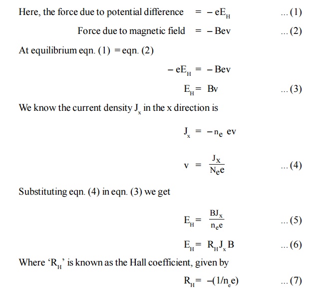
Force due to the potential difference = eEH .. (8)
[Since hole is considered to be an electron with same mass but positive charge negative sign is not included].
At equilibrium eqn. (7) = eqn . (8)
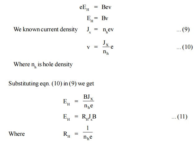
Equation (11) represents the hall coefficient and the positive sign indicates that the Hall field is developed in the positive y direction.
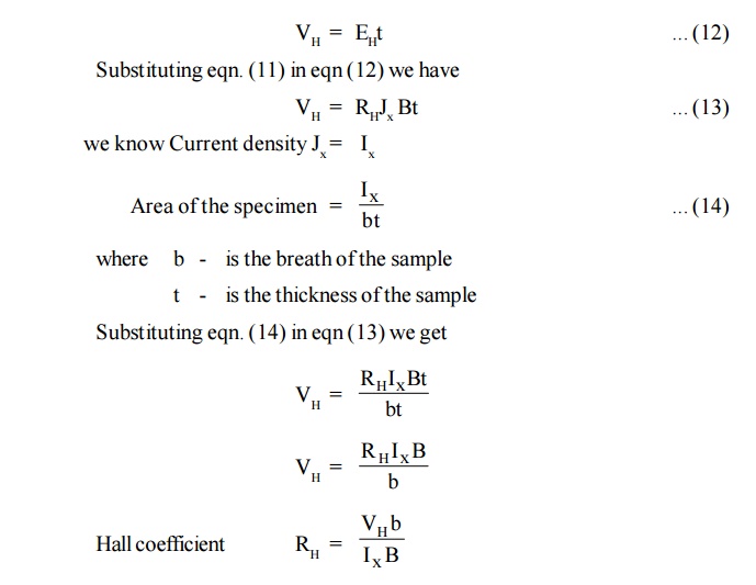
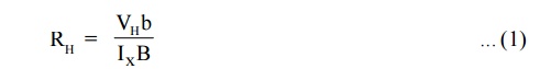
16.4 Hall Coefficient Interms of Hall Voltage
Half coefficient (RH) is defined as the Hall field developed per unit current density per unit applied magnetic field.
If the thickness of the sample is‘t’ and the voltage developed is ‘VH’ then Hall voltage
16.5 Experimental Determination of Hall Effect
A semiconductor slab of thickness ‘t’ and breadth ‘b’ is taken and current is passed using the battery as shown in Figure.
The slab is placed between the pole of an electromagnet so that current direction coincides with x-axis and magnetic field coincides with z-axis. The hall voltage (VH) is measured by placing two probes at the center of the top and bottom faces of the slab (y-axis).
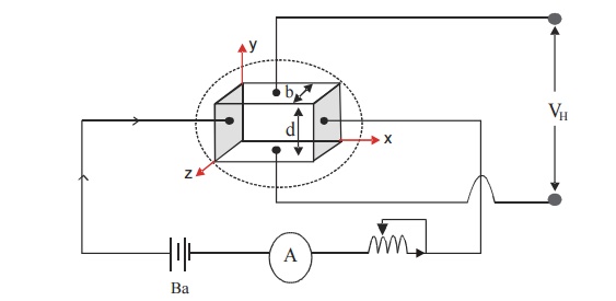
Fig. 2.15 Experimental setup for Hall effect
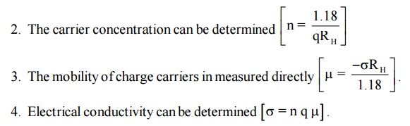
If B is magnetic field applied and the VH is the Hall voltage produced, then the Hall coefficient can be calculated from the formula
Mobility of Charge Carriers
In general the hall co-efficient can be written as
The above expression is valid only for conductors where the velocity is taken as the drift velocity. But for semiconductors velocity is taken as average velocity so RH for an ‘n’ type semiconductor is modified as
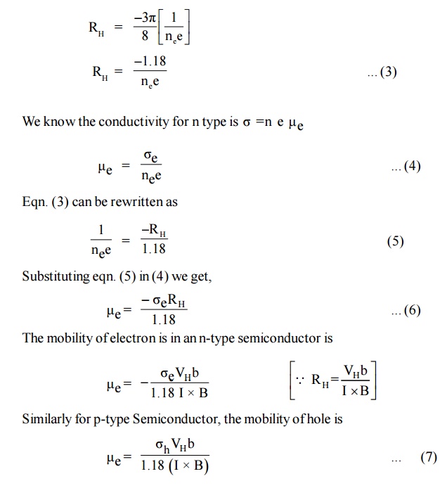
Thus by finding hall voltage, hall coefficient can be calculated and thus the mobility of the charge carriers can also be determined.
16.6 Application of Hall Effect
1. The sign (N-type (or ) P-type) of charge carriers can be determined.
It can be used to determine whether the given material is metal, insulator, or semiconductor and the type of the semiconductor.
It can be used to determine the power flow in an electromagnetic wave.
Related Topics