Chapter: Physics : Semiconducting Materials
Semiconducting Materials
SEMICONDUCTING MATERIALS
1
Introduction
1.1.
Properties of Semiconducting materials
1.2.
Elemental and Compound semiconductors
2
Intrinsic Semiconductors – Electrons and Holes
3
Carrier Concentration in an Intrinsic Semiconductor
3.1.
Density of Electrons
3.2.
Density of Holes
3.3.
Density of intrinsic Carrier Concentration
3.4.
Fermi Energy Level
3.5.
Electrical Conductivity
3.6.
Determination of Band gap in intrinsic semiconductor
4
Extrinsic Semiconductor
4.1.
n- type Semiconductor
4.2.
p- type Semiconductor
5
Carrier Concentration and Fermi level Calculation in n- type Semiconductor
5.1.
Fermi energy level
5.2.
Density of electron Concentration
5.3.
Electrical Conductivity
5.4.
Variation of carrier concentration with temperature in n – type semiconductor
6
Carrier Concentration and Fermi level Calculation in p- type Semiconductor
6.1.
Carrier Concentration
6.2.
Fermi Energy level
7
Variation of carrier concentration with temperature in P- type Semiconductor
8
Hall Effect
8.1.
Statement
8.2.
Theory
8.3.
Calculation of Hall Coefficient
8.4.
Applications of Hall Effect
1 INTRODUCTION
Based on electrical resistance
The resistivity of a
semiconductor is lesser then an insulator but more than that of a conductor. It
is in the order of 10-4 to 0.5 ohm metre.
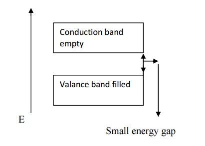
Based on energy band
A semiconductor has nearly empty
conduction band and almost filled valance band with very small energy gap (≈
1eV).
1.1. GENERAL PROPERTIES OF
SEMICONDUCTORS
They are
formed by covalent bonds.
They have an
empty conduction band at 0K They have almost filled valance band
They have
small energy gap They posses crystalline structure
They have
negative temperature co efficient of resistance
If the
impurities are added to a semiconductor, its electrical conductivity increases.
Similarly, if the temperature of the semiconductor increased, its electrical
conductivity increases.
1.2. ELEMENTAL AND COMPOUND
SEMICONDUCTORS
The semiconductors are classified mainly
into two types based on composition of materials.
Elemental
semiconductors
Compound
semiconductors
Elemental semiconductors
These semiconductors are made from a
single element of fourth group elements of the periodic table.
They are also known as indirect band gap
semiconductors
Example –Germanium, silicon
Compound semiconductors
Semiconductors which
are formed by combining third and fifth group elements or second and sixth
group elements in the periodic table are known as compound semiconductors.
These compound semiconductors are also known as direct band gap semiconductors.
Example –1. Combination of third and
fifth group elements
Gallium
phosphide (GaP)
Gallium
arsenide (GaAs)
Indium
phosphide (InP)
Indium
arsenide (InAs)
2. Combination
of second and sixth group elements Magnesium oxide (MgO)
Magnesium
silicon (MgSi) Zinc oxide (ZnO)
Zinc sulphide
(ZnS)
Types of semiconductors
Based on the purity semiconductors are
classified in to the following two types. Intrinsic semiconductors
Extrinsic
semiconductors
Intrinsic semiconductors
A semiconductor in
extremely pure form, without the addition of impurities is known as intrinsic
semiconductors. Its electrical conductivity can be changed due to thermal
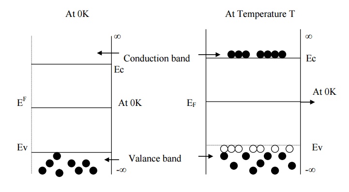
excitation.
At 0K the valance band
is completely filled and the conduction band is empty. The carrier
concentration (i.e) electron density (or) hole density increases exponentially
with increase in temperature.
Extrinsic semiconductors
A semiconductor in
extremely impure form, with the addition of impurities is known as extrinsic semiconductors.
2 INTRINSIC SEMICONDUCTORS –ELECTRONS
AND HOLES
We know that, at 0K intrinsic pure
semiconductor behaves as insulator. But as temperature increases some electron
move from valance band to conduction band as shown in fig. therefore both
electrons in conduction band and holes in valance band will contribute to
electrical conductivity. Therefore the carrier concentration (or) density of
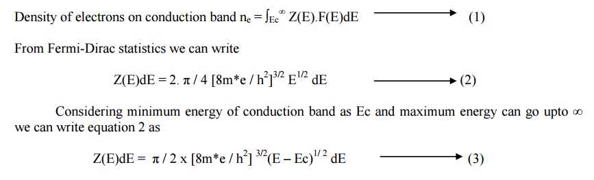
electrons (ne) and holes (nh) has to be calculated.
Assume that electron in
the conduction band as a free electron of mass m*e and the hole in
the valance band behave as a free particle of mass m*h. The
electrons in the conduction band have energies Lying from Ec
to ∞ and
holes-∞intotheEv valanceasshownb
Ec represents the lowest energy level of conduction band Ev represents the
highest energy level of the valance band.
3. CARRIER CONCENTRATION IN AN INTRINSIC
SEMICONDUCTOR
3.1. DENSITY OF ELECTRONS IN CONDUCTION
BAND
We know Fermi function, probability of
finding an electron in a given energy state is
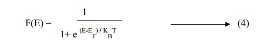
Substituting equation 4 & 3 in
equation 1 we have Density of electrons in conduction band within the limits Ec
to ∞ as
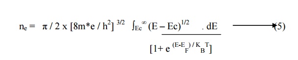
Since to move an
electron from valavce band to conduction band the energy required is greater then
4 KBT (i.e) E –EF
>>KBT (or) (E - EF) / KBT >>1
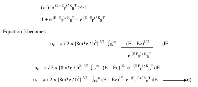
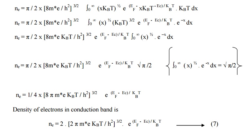
Let us assume that E –Ec = x KBT
Or E = Ec + x KBT
Differentiating we get dE = KBT. dx,
Limits: when
E = Ec; x = 0
When
E = ∞;
x = ∞
Limits are 0 to ∞
Equation 6 can be written as
3.2.
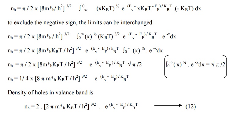
DENSITY OF HOLES IN VALANCE BAND
We know F(E) represents the probability
of filled states. As the maximum probability 1, the probability of un filled
states will be [1 –F(E)].
Example,
if F(E) = 0.8 then 1 –F(E) = 0.2
(i.e) 80% chance of finding an electron in valance
band and 20% chance of finding a hole in valance band.
Let the maximum energy in valance band
be Ev and the minimum energy be -∞. Theref density of hole in valance band nh
is given by
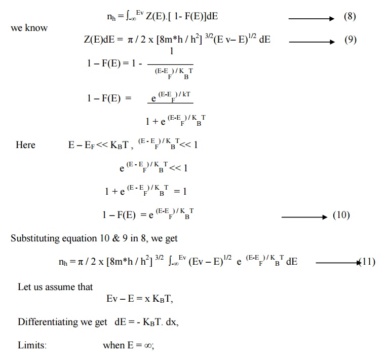
Let us assume that
Ev –E = x KBT,
Differentiating we get dE = - KBT. dx,
Limits: when E = ∞;
When Ev –(-∞) =
x; x = ∞
when E = Ev; x = 0
Limits
are ∞ to 0
Equation 11 becomes
3.3. DENSITY OF INTRINSIC CARRIER
CONCENTRATION
In an intrinsic semiconductor, the
concentration of electrons in the conduction band is equal to the concentration
of holes in the valance band.
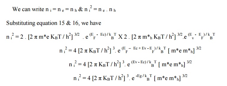
Where Ec –Ev = Eg is the forbidden
energy gap.
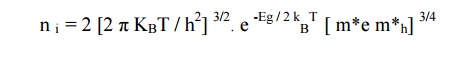
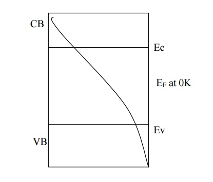
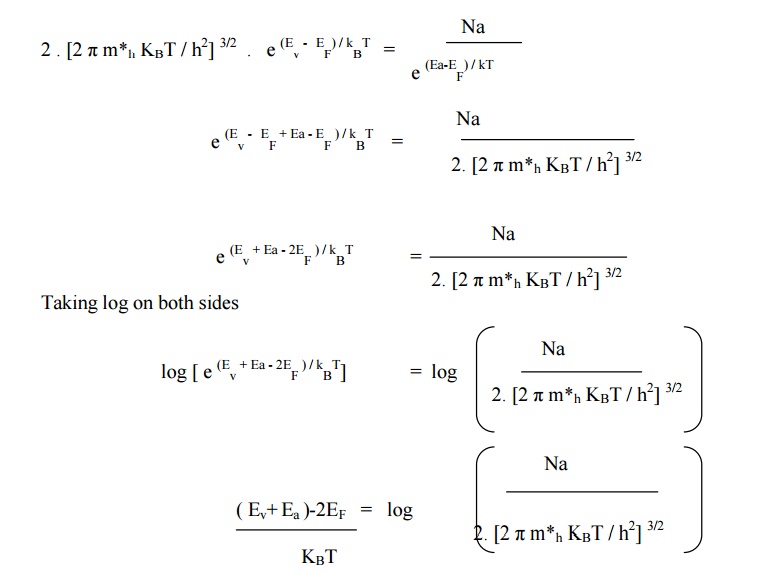
3.4. FERMI ENERGY LEVEL
For an intrinsic semiconductor number of
electrons (i.e) electron density will be the same as that of the number of
holes (i.e) hole density.
(i.e) n e = n h
Equating equations 7& 12
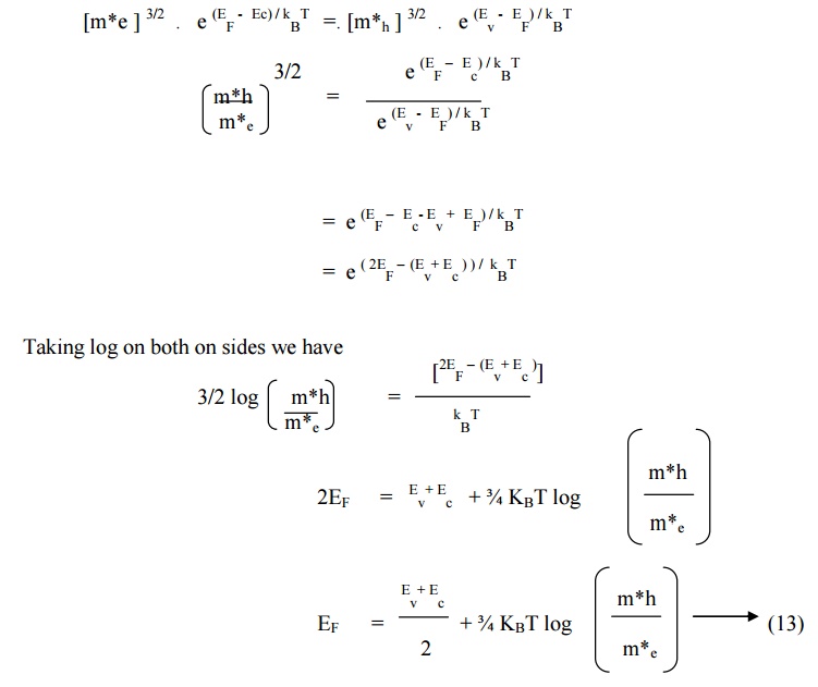
If m*h = m*e, then log m*h / m*e = 0 since log 1 = 0
(i.e)
the Fermi energy level lies in the midway between Ec and Ev as shown fig (since
at 0K, T = 0).
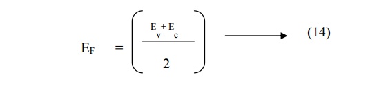
But in actual case m*h m*e
and the Fermi energy level slightly increases with increase in temperature as
shown in fig.
Mobility
When an electric field
is applied to a semiconductor, the charge carrier namely electrons and holes
attain drift velocity Vd. The drift velocity attained by the charge
carrier is proportional to electric field strength E.
Drift velocity Vd is proportional to E
(i.e) Vd α E
Vd
= μ
E
Where μ is proportionality constant and it is known as the mobility of the charge carrier being considered. Mobility μ is defined as the velocity of a charge carrier produced unit field strength.
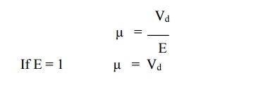
The electron and hole nobilities are denoted by the symbols μe and μh .
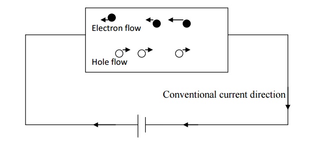
3.5.ELECTRICAL CONDUCTIVITY
Electrical conductivity
of a semiconductor is different from that of a conductor. The charge carriers
in a conductor are electrons. In the case of a semiconductor, both electron and
holes are charge carriers.
On the basis of free electron theory of
solids, the electrical conductivity of metal is given by
σ =μ ne
----(1)
Using the equation 1, the electrical
conductivity of a semiconductor due to electrons in the conduction band is
given by
σe = n e e μ e -----(2)
Where n e is the number of
electrons per unit volume; e is the charge of an electron
μe
is the electron mobility.
Similarly, the electrical conductivity
of a semiconductor due to holes in the valance band is given by
σh = n h e μ
h ----(3)
where n h - is the hole
density in the valance band; e - is the charge of a hole
μh –is the hole mobility
Therefore the total electrical
conductivit conductivities due to electrons and holes.
σi = σ e + σ h ---------(4)
Substituting equations 2& 3 in the
equation 4,
We have
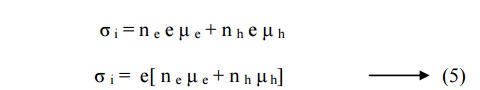
For an intrinsic semiconductor, the
number of electrons in the conduction band is equal to the number of holes in
the valance band,
(i.e) n e = n h =
n i
Where n i is the intrinsic carrier concentration.
Hence, the electrical conductivity of an intrinsic
semiconductor is given by
σi = e[ n i μe
+ n i μh]
Thus, the electrical conductivity
depends upon the negative exponential of the forbidden energy gap Eg and on the motilities’ of both electron
and holes.
3.6.
BAND GAP DETERMINATION
Electrical conductivity of an intrinsic semiconductor
is given by
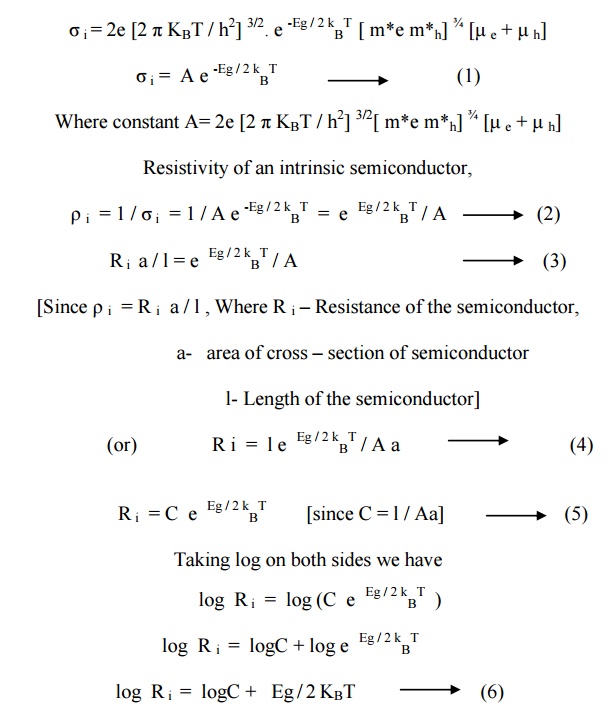
This equation (6) is
similar to the equation of a straight line, y = mx + c
In equation (6), y = log R; x = 1 /
T; m = Eg / 2 KBT and c =
logC
From the
equation 6, it
is noted that by measuring
the resistance of
an intrinsic semiconductor at
different temperatures, its forbidden energy gap Eg can be determined.
If a graph is drawn between log R and 1
/ T, the value of Eg is determined from the slope of a straight line.
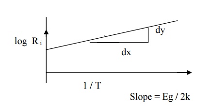
Slope = Eg / 2k
Eg = 2k X slope ----(7)
From the graph slope = dy / dx
Substituting the expression for the slope in
equation (7), we have
Eg
= 2k dy / dx
Where, k is the Boltzmann’s constant.
4 EXTRINSIC SEMICONDUCTOR
In a semiconducting material, if the
charge carriers originate from impurity atoms added to the original material,
then this type of semiconductor is called extrinsic or impure semiconductor. It
is also known as doped semiconductor.
Doping
The method of adding
impurities to a pure semiconductor is known as doping and impurity added is
called doping agent or dopant.
The addition of
impurities will increase the number of free electrons and holes in a
semiconductor and hence increases its electrical conductivity.
Advantages of extrinsic semiconductor
Conductivity
is high.
Conductivity
can be controlled to any desired value through the control of doping
concentration.
Conductivity
is not a function of temperature.
Types of extrinsic semiconductor
The
extrinsic semiconductors are classified into two types based on the type of
impurity added.
(i). n –type semiconductor
(ii). P –type semiconductor
4.1.
N –TYPE SEMICONDUCTOR
When a small amount of
pentavalent impurity (group V element) is added to a pure semiconductor, it
becomes a n –semiconductor.. such impurities are known as donor impurities
because they donate the free electrons to the semiconductor crystal.
A pentavalent
impurity (arsenic) having
five valance electrons
is added to
a pure
semiconducting material having four valance
electrons (silicon or germanium).
The
four valance electrons of the impurity atoms bond with four valance electrons
of the
semiconductor atom and remaining 1 electron of the
impurity atom is left free as shown fig.
Therefore number of free electrons increases, as the
electrons are produced in excess, they the majority charge carrier in n –type
semiconductor and holes are the majority charge carriers.
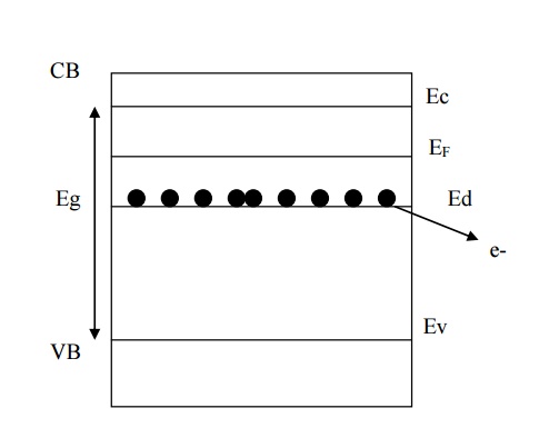
Since electrons are donated in this type of
semiconductor the energy level of these donated electrons is called donor
energy level (Ed) as shown in fig.
Ed is very close to
conduction band and hence even at room temperature the electrons are easily
excited to conduction band. The current flow in this type of semiconductor is
due to electrons.
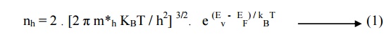
4.2. P –TYPE SEMICONDUCTOR
P –type semiconductor
is obtained by doping an intrinsic semiconductor with trivalannt (3 electrons
in valance band)impurity atoms like boron, gallium, indium etc.,
The three valance
electrons of the impurity atom pairs with three valence electrons of the
semiconductor atom and one position of the impurity atom remains vacant, this
is called hole as shown in fig
Therefore the number of
holes increased with impurity atoms added to it. Since holes are produced in
excess, they are the majority charge carriers in p –type semiconductor and
electrons are the minority charge carriers.
Since the impurity can accept the
electrons this energy level is called acceptor energy level (Ea) and is present
just above the valence band as shown in fig.
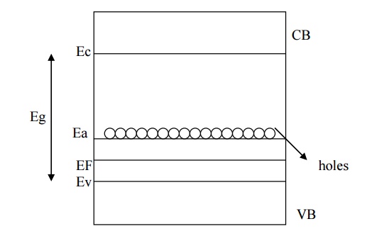
Here the current
conduction is mainly due to holes (holes are shifted from one covalent bond to
anther).
5 CARRIER CONCENTRATION IN N –TYPE
SEMICONDUCTOR
5.1. FERMI ENERGY LEVEL
The energy band
structure of n –type semiconductor is shown in fig. At 0 K, EF will
lie exactly between Ec and Ed, but even at low temperature some electrons may
go from Ed to Ec. Let us assume that Ec –EF > KBT.
Then the density of electrons in conduction band can be written as
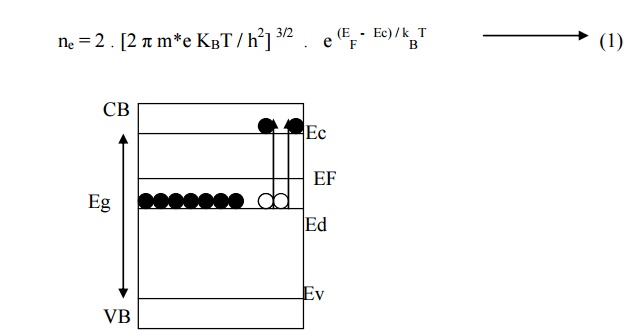
Let Nd be the number of donor
energy levels per cm 3 (i.e) density of state Z(Ed) dE. If some
electrons donated from donor energy level to conduction band say for example if
two electrons goes to conduction band then two vacant sites (holes) will be
created in Ed levels.
Thus in general we can write the density
of holes in donor energy level as
N(Ed) dE = Z(Ed)
dE .(1 –F(Ed))
(i.e) n h = Nd .(1
–F(Ed)) ---(2)
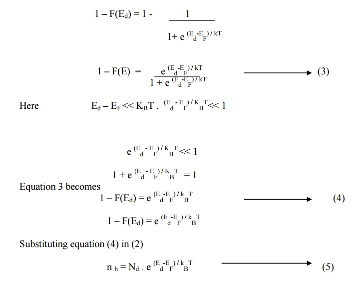
At equilibrium condition
Number of electrons per unit volume in
conduction band (electron density) = Number of holes per unit volume in
conduction band (hole density)
Equating equation (1) and equation (5)
we get
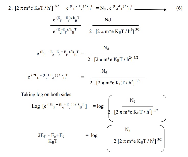
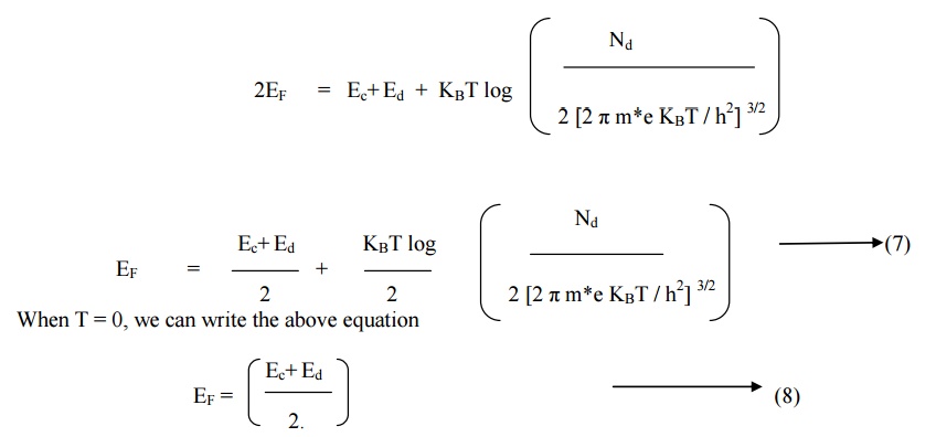
Equation (7) shows that, at 0K, EF
will lie expertly in the midway between Ec and Ed.
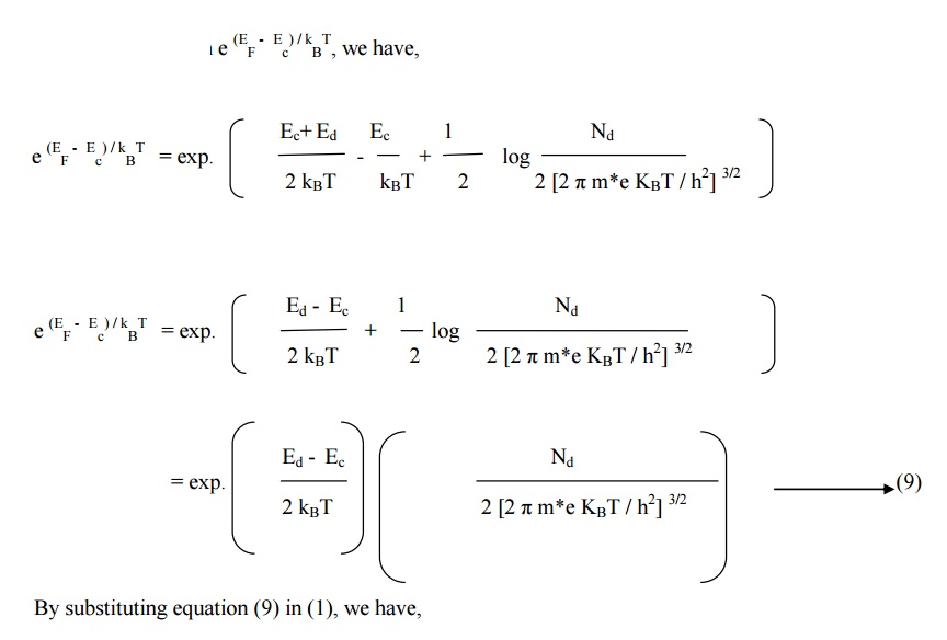
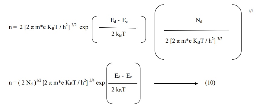
5.2 DENSITY OF ELECTRON CONCENTRATION
(n)
By substituting Ef
value from equation (7) into expression
5.3ELECTRICAL
CONDUCTIVITY
We
know that electrical conductivity in semiconductor is given by
σn
= n e e μ e +n h e μ h
where
μh=0
σn = n e e μ
e
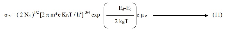
This equation represent the electrical
conductivity of n –type semiconductor.
5.4
VARIATION OF CARRIER CONCENTRATION WITH
TEMPERATURE IN N – TYPE SEMICONDUCTOR
When the temperature increased some
electrons in Ed level may be shifted to conduction band and hence some vacant
sites will be created in Ed levels. Therefore the Fermi level shifts down to
separate that empty levels and the filled valance band level as shown in fig.
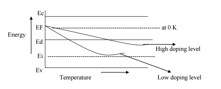
From the above figure
it can be seen that for the same temperature, if the impurity atoms (i.e)
doping level is increased, the electron concentration increases and hence Fermi
level increases.
6 CARRIER CONCENTRATION AND FERMI LEVEL
IN P –TYPE SEMICONDUCTOR
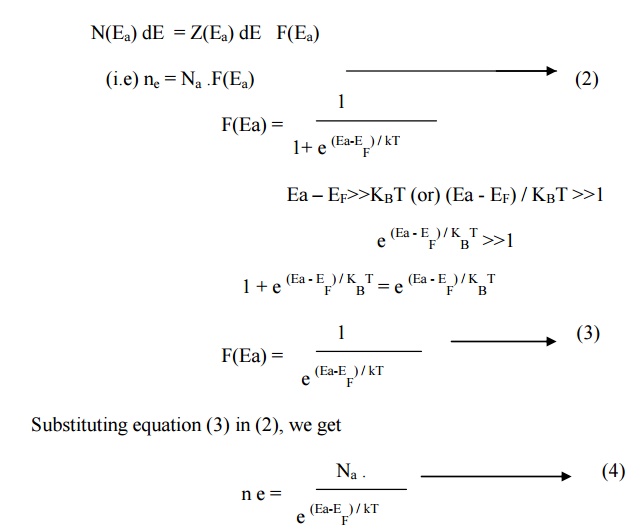
6.1. CARRIER CONCENTRATION
For p –type at absolute
zero EF will be exactly between Ea and Ev. At low temperature some electron
from valence band fills the holes in the acceptor energy level as shown in
figure.
We know the density of holes in the
valence band,
Let Na be the number of acceptor energy levels per
cm 3 which has energy Ea above valence band. If some electrons are accepted by
acceptor energy levels from the valence band, say for example
if two electrons are accepted to fill the hole sites
in the acceptor levels, then two holes will be created in the valence band as
shown in fig .
Therefore in general the electron density in the
acceptor energy level can be written as
N(Ea) dE = Z(Ea) dE F(Ea)
At equilibrium condition
Number of electrons per unit volume in conduction
band (electron density) = Number of holes per unit volume in conduction band
(hole density)
Equating equation (1) and equation (4) we get
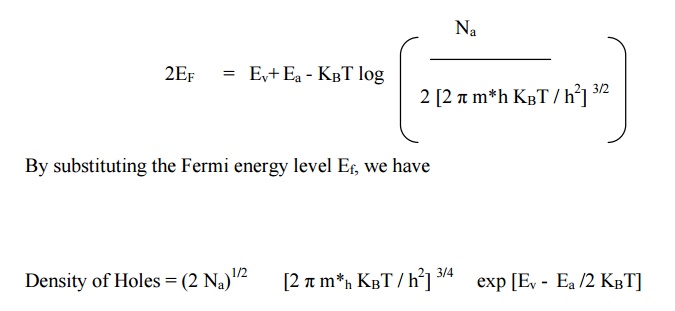
6.2. FERMI ENERGY LEVEL
At 0K, when T= 0 we can write equation (5)
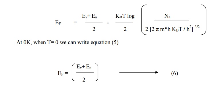
7 VARIATION OF FERMI
LEVEL WITH TEMPERATURE AND IMPURITY CONCENTRATION IN P –TYPE SEMICONDUCTOR
When the temperature is
increased, some of the electrons in the valence band will go to the acceptor
energy level by breaking up the covalent bonds and hence Fermi energy level
shifted upward direction for doping level of Nd = 10 21 atoms / m3
as shown in figure.
From the figure it can be seen that for the same
temperature, if the impurity atoms (i.e) doping level is increased say Nd = 10 24
atoms /m3, the hole concentration increases and hence the Fermi
level decreases.
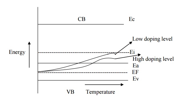
Therefore at low
temperature the Fermi energy level may be increased up to the level of
intrinsic energy level (Ei).
8 HALL EFFECT:
Measurement of
conductivity will not determine whether the conduction is due to electron or
holes and therefore it will be very difficult to distinguish between p –type
and n- type semiconductors.
Therefore Hall Effect
is used to distinguish between the two types of charge carriers and their
carrier densities and is used to determine the mobility of charge carriers.
8.1.STATEMENT
When a conductor (metal or semiconductor) carrying
current (I) is placed perpendicular to a magnetic field (B), a potential
difference (electric field) is developed inside the conductor in a direction
perpendicular to both current and magnetic field. This phenomenon is known as
Hall Effect and the voltage thus generated is called Hall voltage.
8.2. THEORY
Hall effect in n- type semiconductor
Let us consider a n-type semiconductor material in
the form of rectangular slab. In such a material current flows in X –direction
and magnetic field B applied in Z- direction. As a result, Hall voltage is
developed along Y –direction as shown in figure.
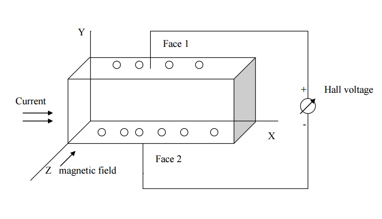
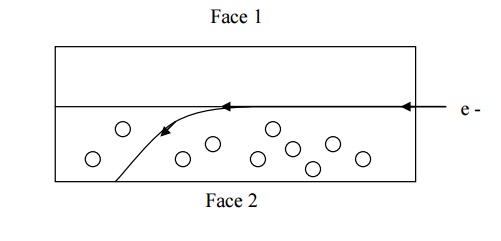
Since the direction of
current is from left to right the electrons moves from right to left in
X-direction as shown in fig
Now due to magnetic
field applied the electron moves towards downward direction with velocity v and
cause negative charge to accumulate at face (1) of the material as shown in
fig. therefore the potential difference is established between the face (2) and
face (1) of the specimen which gives rise to EH in the negative Y direction.
Here, the force due to
potential difference = -e EH ---(1)
Force due magnetic
field = - Bev ---(2)
At equilibrium equation
(1) = equation (2)
-e EH = -
Bev
EH = Bv ---(3)
We know the current
density Jx in the X- direction is
Jx = -ne ev
v = - Jx / ne
e ---(4)
Substituting equation
(4) in equation (3) we get
EH
= - B Jx / ne e
----(5)
EH
= RH . Jx . B ----(6)
Where RH is
known as the Hall co –efficient, is given by
RH = - (1 /
ne e) ----(7)
The negative sign indicates that the field is
developed in the negative Y –direction.
Hall effect in p –type semiconductor
Let us consider a p
–type semiconducting material for which the current is passed along X –
direction from left to right and magnetic field is applied along Z –direction
as shown in fig. since the direction of current is from left to right, the
holes will also move in the same direction as shown in fig.
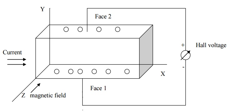
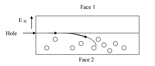
Now due to magnetic
field applied the holes moves towards downward direction with velocity v and
accumulates at the face (1). A potential difference is established between face
(1) and (2) in the positive Y - direction.
Here, the force due to
potential difference = -e EH ----(8)
Force due magnetic
field = Bev ----(9)
At equilibrium equation
(1) = equation (2)
e EH = Bev
EH = Bv --------------(10)
We know the current
density Jx in the X- direction is
Jx = nh ev
v = Jx / nh
e -----------(11)
Substituting
equation (4) in equation (3) we get
EH
= B Jx / nh e
EH
= RH . Jx . B
Where RH is
known as the Hall co –efficient, is given by
RH = (1 / nh
e) ----(12)
The
positive sign indicates that the field is developed in the positive Y
–direction
Hall
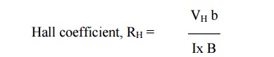
coefficient in terms of hall voltage
If the thickness of the
sample is t and the voltage developed is VH, then
Hall voltage VH
= EH .t ---((13))
Substituting equation
(6 )in equation (13), we have
VH = RH
Jx B .t ----(14)
If
b is the width of the sample then
Area
of the sample = b.t
Current density = Jx =
Ix / bt -----(15)
Substituting equation
(15) in equation (14) we get
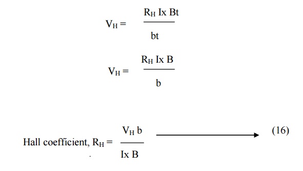
The sign for VH will be
opposite for n and p type semiconductors.
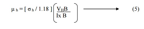
Mobility
of charge carriers
We
know that Hall coefficient,
RH
= - (1 / ne e)
The above expression is valid only for
conductors where the velocity is taken as the drift velocity.
But for semiconductor
velocity is taken as average velocity so RH for n- type semiconductor is
modified as
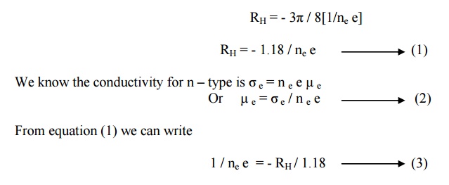
Substituting equation (3) in equation (2) we get
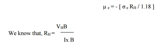
For n –type
semiconductor, the mobility of electron is
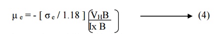
Similarly for p –type
semiconductor, the mobility of hole is
8.3. EXPERIMENTAL DETERMINATION OF HALL
EFFECT
A semiconducting
material is taken in the form of a rectangular slab of thickness t and breadth
b. A suitable current Ix ampere is passed through this sample along X- axis by
connecting it to a battery.
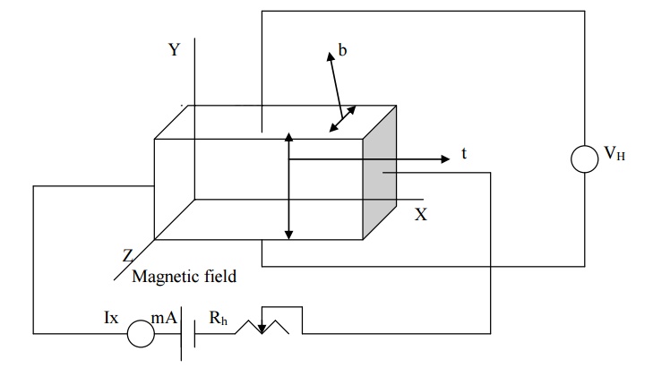
This sample is placed
in between two poles of an electro magnet such that magnetic field is applied
along Z –axis.
Due to Hall Effect,
Hall voltage (VH) is developed in the sample. This voltage measured
by fixing two probes at the centers of the bottom and top faces faces of the
sample. By measuring Hall voltage, Hall coefficient is determined from the
formula
From
the hall coefficient, carrier concentration and mobility can be determined.
8.4. APPLICATIONS OF
HALL EFFECT
It is used to determine
whether the material is p-type or n-type semiconductor. (ie ) if RH is negative
then the material n-type. If the RH is positive then the material p-type.
It is used to find the
carrier concentration
It is used to find the mobility of charge carriers μe, μh.
It is used to find the
sign of the current carrying charges.
It is used to design
magnetic flux meters and multipliers on the basis of Hall voltage. It is used
to find the power flow in an electromagnetic wave.
Related Topics