Chapter: Physics : Semiconducting Materials
Important Questions and Answers: Semiconducting Materials
SEMICONDUCTING MATERIALS
1.
What are elemental semiconductors? Give some important elemental
semiconductors.
Elemental semiconductors are made from
single element of the forth group elements of the periodic table.
It
is also known as indirect band gap semiconductor.
Example:
Important
elemental semiconductors germanium and silicon.
2.What
are the properties of semiconductors?
(i) They
are formed by covalent bond.
(ii) They
have empty conduction
band.
(iii)They
have almost filled valance band.
(iv)These
materials have comparatively narrow energy gap.
3.
Mention any four advantages of semiconducting materials.
(i) It can behave as insulators at 0K and as conductors at high temperature.
(ii) It possess some
properties of both conductors and insulators.
(iii) On
doping we can produce both N and P-type Semiconductors with charge carriers of
electrons and holes respectively.
(iv)It
possess many applications in electronic field such as manufacturing of diodes,
transistors, LED’s,IC etc.
4. What
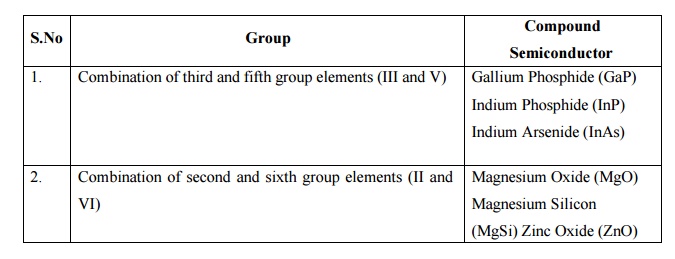
are compound semiconductors? Give some important compound semiconductors.
Semiconductors which are formed by
combining third and fifth elements or second and sixth group elements in the
periodic table are called compound semiconductors.
Important
compound semiconductors are

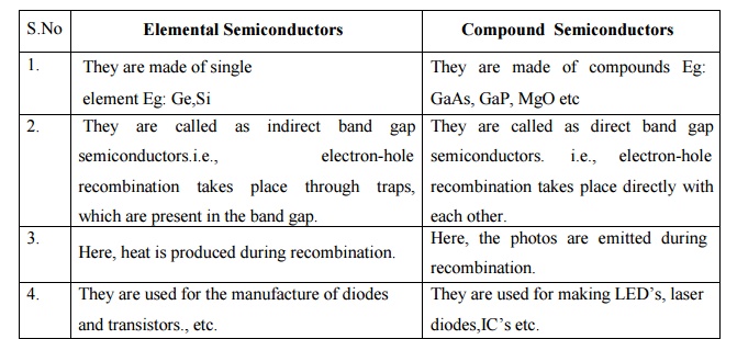
5. What are the differences between
elemental semiconductors and compound semiconductors?

S.No Elemental Semiconductors
1.
They are made of single element Eg: Ge,Si
2.
They are called as indirect band gap semiconductors.i.e., electron-hole
recombination takes place through traps, which are present in the band gap.
3.
Here, heat is produced during recombination.
4.
They are used for the manufacture of diodes and transistors., etc.
Compound Semiconductors
They
are made of compounds Eg: GaAs, GaP, MgO etc
They
are called as direct band gap semiconductors.i.e., electron-hole recombination
takes place directly with each other.
Here,
the photos are emitted during recombination.
They
are used for making LED’s, laser diodes,IC’setc.
6. What is Fermi level in a
semiconductor?
Fermi level in a
semiconductor is the energy level situated in the band gap of the
semiconductor. It is exactly located at the middle of the band gap in the case
of intrinsic semiconductor.
7. Define Hall-effect and Hall voltage.
When a conductor (metal
or semiconductor) carrying a current (I) is placed in a transverse magnetic
field (B),a potential difference (electric field) is produced inside the
conductor in a direction normal to the directions of both the current and
magnetic field.
This phenomenon is known as Hall-effect and
the generated voltage is called Hall-voltage.
Hall field per unit current density per unit
magnetic induction is called hall coefficient.
8. Mention the applications of Hall
Effect.
It
is used to,
i.
Find type of semiconductor.
ii.
Measure carrier concentration.
iii.
Find mobility of charge
carrier.
iv.
Measure the magnetic flux density using
a semiconductor sample of known Hall coefficient.
9. What
is a semiconductor?
Semiconductor is a
special class of material which behaves like an insulator at o K and acts
conductor at temperature other than 0K. Its resistivity lies in between a
conductor and an insulator.
10. What is an intrinsic semiconductor?
Semiconductor in an
extremely pure form (without impurities) is known as intrinsic semiconductor.
11. What is an
extrinsic semiconductor?
A semiconducting
material in which impurity atoms added
(doped) to the material to modify its conductivity is known as extrinsic
semiconductor or impurity semiconductor.
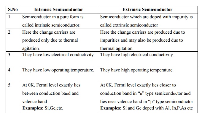
12. What is meant by intrinsic semiconductor
and extrinsic semiconductor? What are the
differences
between intrinsic and extrinsic semiconductor.

S.No Intrinsic Semiconductor
1.
Semiconductor in a pure form is called intrinsic semiconductor.
2.
Here the change carriers are produced only due to thermal agitation.
3.
They have low electrical conductivity.
4.
They have low operating temperature.
5.
At 0K, Fermi level exactly lies between conduction band and valence band.
Examples:
Si,Ge,etc.
Extrinsic Semiconductor
Semiconductor
which are doped with impurity is called extrinsic semiconductor
Here
the change carriers are produced due to impurities and may also be produced due
to thermal agitation.
They
have high electrical conductivity.
They
have high operating temperature.
At
0K, Fermi level exactly lies closer to conduction band in n”“ypetsemiconductor
and lies near valence band in “p”type semiconductor.
Examples:
Si and Ge doped with Al, In,P,As etc
13.
What is an n-type semiconductor?
When a small amount of pentavalent impurity
is added to a pure semiconductor, it becomes extrinsic or impure semiconductor
and it is known as n-type semiconductor.
14.
What is a p-type semiconductor?
When a small amount of trivalent
impurity is added to a pure semiconductor, it becomes extrinsic or impure
semiconductor and it is called p-type semiconductor.
15.
What is meant by doping and doping agent?
The technique of adding impurities to a
pure semiconductor is known as doping and the added impurity is called doping
agent.
16.
What is meant by donor energy level?
A
pentavalent impurity when doped with an intrinsic semiconductor donates one
electron which produces an energy level called donor energy level.
17.
What is meant by acceptor energy level?
A trivalent impurity when doped with an
intrinsic semiconductor accepts one electron which produces an energy level
called acceptor energy level.
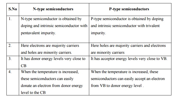
18.
Compare n-type and p-type semiconductors.

S.No N-type semiconductors
1.
N-type semiconductor is obtained by doping and intrinsic semiconductor with
pentavalent impurity.
2.
Here electrons are majority carriers and holes are minority carriers.
3.
It has donor energy levels very close to CB
4.
When the temperature is increased, these semiconductors can easily donate an
electron from donor energy level to the CB
P-type semiconductors
P-type
semiconductor is obtained by doping and intrinsic semiconductor with trivalent
impurity.
Here
holes are majority carriers and electrons are minority carriers
It
has acceptor energy levels very close to VB.
When
the temperature is increased, these semiconductors can easily accept an
electron from VB to donor energy level .
19.
Define impurity range, exhaustion range and intrinsic range in n-type
Semiconductors.
Impurity range:
This range is due to the transfer of electrons from the donor energy Level to
CB. Here the electron concentration in the CB steadily increases due to
ionization of donor atoms.
Exhaustion range:
When all the electrons are transferred from donor energy level to conduction
band, the electron concentration remains constant over certain temperature and
is called exhaustion range.
Intrinsic range: In
this range the n-type semiconductor practically behaves like the Intrinsic semiconductor.
Therefore if the temperature is increased the electrons concentration in the
conduction band increases rapidly due to the shifting of electrons from valence band to
Related Topics