Chapter: Optical Communication and Networking : Fiber Optic Receiver and Measurements
Receiver Configuration
Receiver Configuration
ü A typical optical receiver is shown in Figure 4.4. The three basic stages of the receiver are a photodetector, an amplifier, and an equalizer.
ü The photo-detector can be either an APD with a mean gain M or a PIN for which M=1.
ü The photodiode has a quantum efficiency h and a capacitance Cd.
ü The detector bias resistor has a resistance Rb which generates a thermal noise current ib(t).
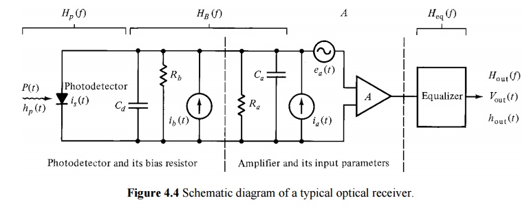
Amplifier Noise Sources:
ü The input noise current source ia(t) arises from the thermal noise of the amplifier input resistance Ra;
ü The noise voltage source ea(t) represents the thermal noise of the amplifier channel.
ü The noise sources are assumed to be Gaussian in statistics, flat in spectrum (which characterizes white noise), and uncorrelated (statistically independent).
The Linear Equalizer:
ü The equalizer is normally a linear frequency shaping filter that is used to mitigate the effects of signal distortion and inter symbol interference (ISI).
ü The equalizer accepts the combined frequency response of the transmitter, the fiber, and the receiver, and transforms it into a signal response suitable for the following signal processing electronics.
ü The binary digital pulse train incident on the photo-detector can be described by
ü Here, P(t) is the received optical power, Tb is the bit period, bn is an amplitude parameter representing the nth message digit, and hp(t) is the received pulse shape.
ü Let the nonnegative photodiode input pulse hp(t) be normalized to have unit area

then bn represents the energy in the nth pulse.
ü The mean output current from the photodiode at time t resulting from the pulse train given previously is
where Ro = hq/hn is the photodiode responsivity.
ü The above current is then amplified and filtered to produce a mean voltage at the output of the equalizer.
Related Topics