Chapter: Optical Communication and Networking : Fiber Optic Receiver and Measurements
Pre Amplifiers
Pre Amplifier
The receiver amplifier are the front end preamplifier. The three basic preamplifier structures are:
(1) Low impedance preamplifier
(2) High impedance preamplifier
(3) Trans impedance preamplifier
Advantages Of Pre-Amplifier
A preamplifier should satisfy the following requirements: low noise level, high bandwidth, high dynamic range, high sensitive and high gain.
1. Low Impedance Preamplifier
· Photo diode operates in to a low impedance amplifier bias or load resistor “Rb” is used to match the amplifier impedance.
· Rb along with the input capacitance of amplifier decides the bandwidth of amplifier.
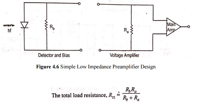
· Low impedance preamplifier can operate over a wide bandwidth but they have poor receiver sensitivity.
· They are used in special short distance application where high sensitivity is not a major concern.
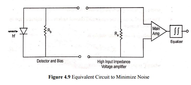
2. High Impedance Preamplifier
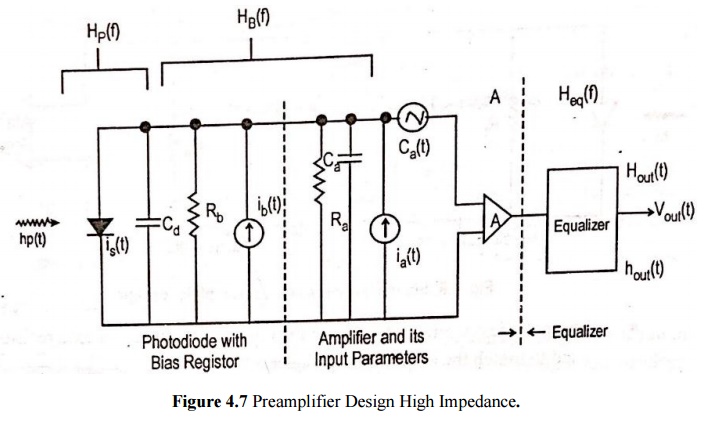
· The second configuration consists of a high input impedance amplifier together with a large detector bias resistor (Ra) in order to reduce the effect of thermal noise.
· In high impedance preamplifier, the goal is to reduce all sources of noise to the absolute minimum. This can be achieved by reducing input capacitance through the selection of low capacitance high frequency devices.
· Selecting detectors with low dark currents.
· Minimizing thermal noise of biasing resistors.
· Using high impedance amplifier with large Rb (eg., a dipolar transistor or a field effect transistor (FET)).
· The high impedance procedure a large input RC time constant, the front end bandwidth is less than signal bandwidth. Thus, the input signal is integrated and equalization techniques must be employed to compensate for this.
High Impedance FET Preamplifier
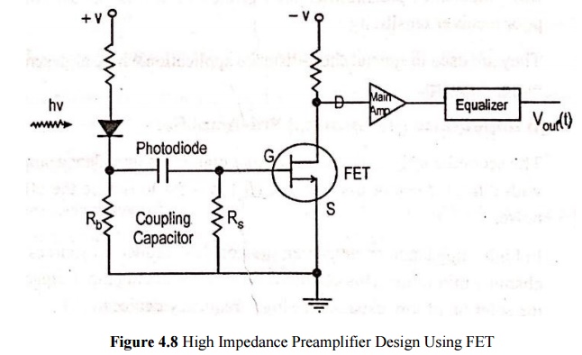
· For giga bit per second data rates, the lowest noise receivers are made using GaAs MOSFET (metal oxide semiconductor field effect transistor) preamplifiers.
· At low frequencies, silicon MOSFETs (metal oxide semiconductor field effect transistors) or JFET are generally used.
Basic Noise Sources in the Circuit are:
· Thermal noise associated with FET channel conductance.
· Thermal noise from load or feedback resistor.
· Shot noise due to gate leakage current.
· A fourth noise source is FET 1/f noise.
· This (1/f noise) was not include in the above analyses beceause it contributes to the overall noise only at very low bit rates.
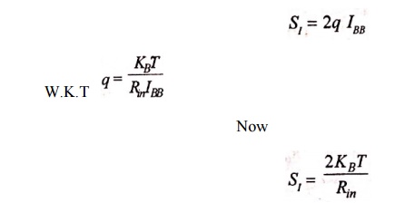
· As he amplifier input resistance is very high, the input current noise spectral density S1 is
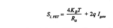
· FET has very large input resistance “Ra” usually greater than 106Ω for practical purpose Re=infinity.

Where Igate is the channel noise factor.
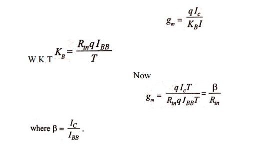
· The thermal noise of the conducting channel resistance is characterized by the transconductance gm.
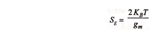
· The voltage noise spectral density is
· Ѓ is a numerical that accounts for thermal noise and gate included noise plus the correlation between these two noises.
· Thermal noise characteristic equation Ω is a very useful figure of merit for a receiver as it measures
· The 1/f noise corner frequency fc is defined as the frequency at which 1/f noise, which dominates the FET noise at low frequencies and has 1/fpower spectrum, becomes equal frequency channel noise described by Ѓ.
· To minimize the noise in a high impedance design, the bias resistor shoud be very large. The effect of this is the detector output signal is integrated by the amplifier input resistance.
· It is compensated by differentiation in the equalizing fitter. This integration differentiation approach is known as the high impedance amplifier design technique.
High Impedance BJT Preamplifier
· The circuit shows a simple bipolar grounded emitter transistor amplifier.
· The input (Rin) of a bipolar transistor is given as
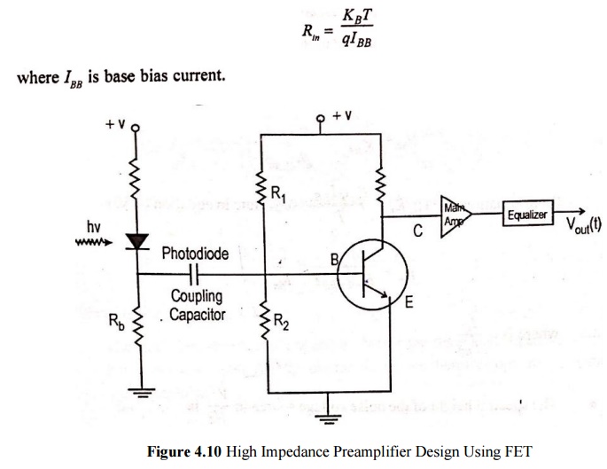
· The amplifier input resistance Ra is given by the parallel combination of the bias resistor R1 and R2 and the transistor input resistance Rin.
· For low noise design (R1+R2>>Rin)
Ra~=Rin
· The spectral density (A2/Hz) of the input noise current source which results from shot noise of the base current is
· The transconductance gm is related to the shot noise and is given by
· The spectral height of the noise voltage source in V2/Hz is
Where kb is the boltzmann’s constant.
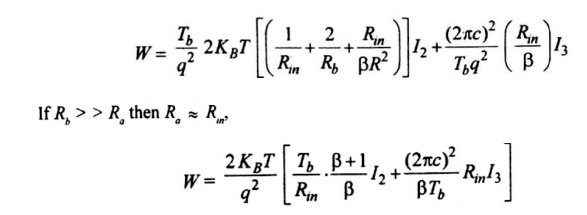
Thermal Noise Characteristic Equation for Receiver Amplifier
· The performance of receiver isexpressed by thermal noise characteristic equation (W).
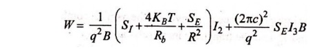
Substituting Rin, S1,SE in characteristic equation
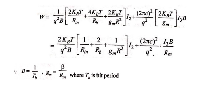
Substitute B & gm in W, We get:
Transimpedance Preamplifier
· The transimpedance amplifier is nothing but the low noise high impedance amplifier with a negative feedback ‘Rf’ resistor, the device therefore operates as a current mode amplifier.
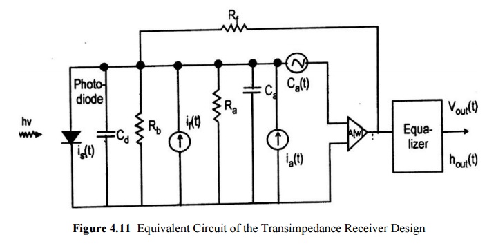
· Transimpedance amplifier design overcomes the drawbacks of high impedance amplifier. Such as
(1) For broadband applications, equalization is required.
(2) It has limited dynamic range.
· The thermal noise characteristic ‘WTZ’ at equalizer output can be found by replacing Rb and Rb’.
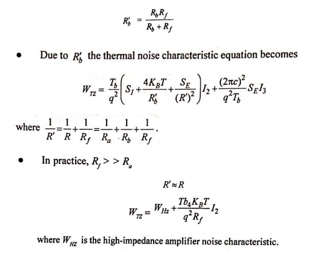
· The thermal noise characteristics are the sum of output noise of a non-feedback amplifier plus the thermal noise associated with the feedback resistance.
Transfer Function of Non-Feedback Amplifier
· The transfer function of non-feedback amplifier is given by
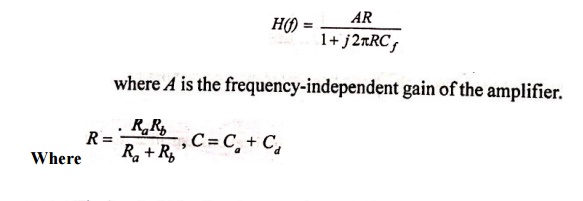
· The bandwidth of non-feedback amplifier is B=1/4RC
Advantages of Transimpedance Amplifier:
(1) Wide dynamic range.
(2) Little or no equalization is required.
(3) Less susceptible to pick up noise, cross talk, EMI.
(4) It is very easily controllable and stable.
(5) Loss sensitivity.
(6) Output resistance is small.
Related Topics