Chapter: Television and Video Engineering : Colour Television Systems
PAL-D Colour System
PAL-D COLOUR SYSTEM
The use of eye as the averaging mechanism for the correct hue is the basis of ‘simple PAL’ colour system. However, beyond a certain limit the eye does see the effect of colour changes on alternate lines, and so the system needs modification.
Remarkable improvement occurs in the system if a delay line is employed to do the averaging first and then present the colour to the eye. This is known as PAL-D or Delay Line PAL method and is most commonly used in PAL colour receivers.
As an illustration of the PAL-D averaging technique, Fig shows the basic circuit used for separating individual U and V products from the chrominance signal. For convenience, both U and V have been assumed to be positive, that is, they correspond to some shade of magenta (purple).
Thus for the first line when the V modulator product is at 90° to the + U axis, the phasor can be expressed as (U + jV). This is called the NTSC line. But on the alternate (next) line when the V phase is switched to – 90°, the phasor becomes (U – jV) and the corresponding line is then called the PAL line.
As shown in Fig. a delay line and, adding and subtracting circuits are interposed between the chrominance amplifier and demodulators.
The object of the delay line is to delay the chrominance signal by almost exactly one line period of 64 μs. The chrominance amplifier feeds the chrominance signal to the adder, the subtractor and the delay line.
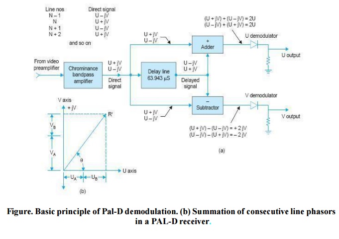
The delay line in turn feeds its output to both the adder and subtractor circuits. The adder and subtractor circuits, therefore, receive the two signals simultaneously. These may be referred to at any given time as the direct line and delay line signals.
For the chosen hue, if the present incoming line is an NTSC line, the signal entering the delay-line and also reaching the adder and subtractor is (U + jV). But then the previous line must have been the PAL line i.e., (U – jV) and this signal is simultaneously available from the delay line. The result is (see Fig. 26.14 (a)) that the signal information of two picture lines, though transmitted in sequence, are presented to the adder and subtractor circuits simultaneously.
The adder yields a signal consisting of U information only but with twice the amplitude (2U). Similarly, the subtraction circuit produces a signal consisting only of V information, with an amplitude twice that of the ‘V ’ modulation product.
To permit precise addition and subtraction of direct and delayed line signals, the delay line must introduce a delay which is equivalent to the duration of an exact number of half cycles of the chrominance signal.
This requirement would not be met if the line introduced a delay of exactly 64 μs. At a
frequency of 4.43361875 MHz the number of cycles which take place in 64 μs are 4.43361875 × 10 6 × 64 × 10 –6 = 283.7485998 Hz, ≈ 283.75 Hz.
A delay line which introduces a delay equal to the duration of 283.5 subcarrier cycles is therefore suitable. This is equal to a time delay of 63.943 μs (1/f sc × 283.5). The addition and subtraction of consecutive line phasors can also be illustrated vectorially by phasor diagrams.
Figure is such a phasor diagram pertaining to the phase error illustration of Fig. The U
and V signals thus obtained are fed to their respective synchronous demodulators for recovery of the colour difference signals Choice of Colour Subcarrier Frequency If the sub-carrier frequency is chosen on the half-line offset basis as is done in the NTSC system, an annoying vertical line-up of dots occurs on certain hues. This is due to phase reversal of the sub-carrier at line frequency.
To overcome this difficulty, a quarter-line offset is given instead and f sc is made an odd multiple of one quarter of the line frequency. For optimum results this is slightly modified by adding 25 Hz to it, to provide a phase reversal on each successive field.
Thus the actual relationship between f sc , f h and f v can be expressed as
f sc = f h
This on substituting the values of f h and f v gives f sc = 4.43361875 MHz.
It may be mentioned that though formation of any dot pattern on the screen must be suppressed by appropriate choice of sub-carrier frequency, it is of low visibility and appears only when colour transmission is received on a monochrome receiver. Since the chrominance signal disappears on grey or white details in a picture, the interference appears only in coloured areas of the scene. All colours appear as shades of grey on a monochrome receiver and thus the dot effect is visible only in those coloured parts of the picture which are reproduced in lighter shades of grey.
Colour Subcarrier Generation
The colour subcarrier frequency of 4.43361875 MHz is generated with a crystal controlled oscillator. In order to accomplish minimum raster disturbance through the colour subcarrier it is necessary to maintain correct frequency relationships between the scanning frequencies and the subcarrier frequency.
It is therefore usual to count down from the subcarrier frequency to twice the line frequency (2f h ) pulses which are normally fed to monochrome sync pulse generators. There are several ways in which frequency division can be accomplished. In the early days of colour television it was necessary to choose frequencies which had low-order factors so that division could take place in easy stages, but such constraints are no longer necessary.
The PAL subcarrier frequency is first generated directly. Then the 25 Hz output obtained from halving the field frequency is subtracted from the subcarrier frequency.
The frequency thus obtained is first divided by 5 and then by 227. Such a large division is practicable by using a chain of binary counters and feeding back certain of the counted down pulses to earlier points of the chain that the count down is changed from a division of 2 8 to a division of the pal coder
The gamma corrected R, G and B signals are matrixed to form the Y and the weighted
colour difference signals. The bandwidths of both (B – Y) and (R – Y) video signals are restricted to about 1.3 MHz by appropriate low- pass filters. In this process these signals suffer a small delay relative to the Y signal. In order to compensate for this delay, a delay line is inserted in the path of Y signal.
The weighted colour difference video signals from the filters are fed to corresponding balanced modulators. The sinusoidal sub-carrier is fed directly to the U modulator but passes through a ± 90° phase switching circuit on alternate lines before entering the V modulator.
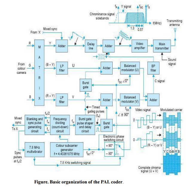
Since one switching cycle takes two lines, the squarewave switching signal from the multivibrator to the electronic phase switch is of half-line frequency i.e., approximately 7.8 KHz.
The double sideband suppressed carrier signals from the modulators are added to yield the quadrature amplitude modulated (Q.A.M.) chrominance (C) signal. This passes through a filter which removes harmonics of the subcarrier frequency and restricts the upper and lower sidebands to appropriate values.
The output of the filter feeds into an adder circuit where it is combined with the luminance and sync signals to form a composite colour video signal. The bandwidth and location of the composite colour signals (U and V) is shown along with the Y signal in Fig Notice that the colour burst signal is also fed to the modulators along with the U and V signals through the adders.
The burst signals are obtained from the circuits that feed the colour subcarrier signal to the two modulators. However, before feeding the burst signals to the U and V adders these are passed through separate burst gates.
Each burst gate is controlled by delayed pulses at f H rate obtained from the frequency dividing circuit. The gating pulses appear during the back porch period.
Thus, during these intervals the (B – Y) i.e., U modulator yields a subcarrier burst along – U while the (R – Y) i.e., V modulator gives a burst of the same amplitude but having a phase of ± 90° on alternate lines relative to the – U phasor. At the outputs of the two modulators, the two burst components combine in the adder to yield an output which is the vector sum of the two burst inputs.
This is a subcarrier sinewave ( ≈ 10 cycles) at + 45° on one line and – 45° on the next line with reference to – U phasor. The colourplexed composite signal thus formed is fed to the main transmitter to modulate the station channel picture carrier in the normal way.
The sound signal after being frequency modulated with the channel sound carrier frequency also forms part of the RF signal that is finally radiated through the transmitter antenna system.
Related Topics