Chapter: Television and Video Engineering : Colour Television Systems
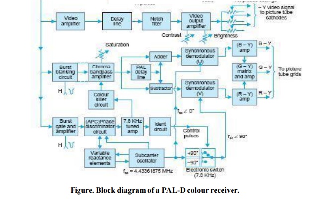
PAL-D Colour Receiver
PAL-D COLOUR RECEIVER
Various designs of PAL decoder have been developed. The one shown in the colour receiver block diagram of Fig. is a commonly used arrangement.
It will be noticed that the general pattern of signal flow is very close to that of the NTSC receiver. Necessary details of various sections of the receiver are discussed.
1. Tuner
It is necessary to maintain local oscillator frequency at the correct value to obtain exact colour burst frequency for proper reproduction of different colours in the picture.
Therefore, colour receiver tuners employ an additional circuit known as automatic frequency tuning (AFT). This circuit actually controls the local oscillator frequency to obtain a picture IF of exactly 38.9 MHz at the converter output.
The discriminator in the AFT circuit measure the intermediate frequency and develops a dc control voltage proportional to the frequency deviations if any.
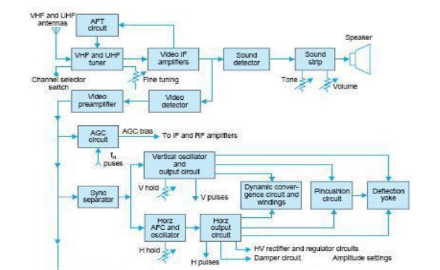
This error voltage is applied to the reactance section of the local oscillator to maintain its frequency at the correct value. More details of AFT are given in the next chapter along with other special circuits.
2. Sound Strip.
· The frequency modulated sound IF signal is processed in the usual way to obtain audio output. The volume and tone controls are associated with the audio amplifier, the output of which feeds into the loudspeaker.
· Thus the sound strip of a colour receiver is exactly the same as in a black and white receiver.
3. AGC, Sync-separator and Deflection Circuits
The AGC and sync-separator circuits function in the same way as in a monochrome receiver. However, the deflection circuits, besides developing normal horizontal and field scanning currents also provide necessary wave-forms for dynamic convergence and pincushion correction.
In addition, pulses from the horizontal output transformer are fed to several circuits in the colour section of the receiver.
4. Luminance Channel
The video amplifier in the luminance channel is dc coupled and has the same bandwidth as in the monochrome receiver. It is followed by a delay line to compensate for the additional delay the colour signal suffers because of limited bandpass of the chrominance. This ensures time coincidence of the luminance and chrominance signals. The channel also includes a notch filter which attenuates the subcarrier by about 10 db. This helps to suppress the appearance of any dot structure on the screen along with the colour picture. The inverted composite video signal available at the output of luminance channel is fed to the junction of three cathodes of the picture tube. This part of the circuit also includes drive adjustment necessary for setting of the black level and obtaining correct reproduction of colours.
5. Colour Signal Processing
The signal available at the output of video detector is given some amplification (video preamplifier) before feeding it to the various sections. All modern receivers use ICs for processing the colour signal. However, for a better understanding, the operation of each stage is described with the help of discrete component circuitry.
(a) Chrominance bandpass amplifier.
As noted previously the chroma bandpass amplifier selects the chrominance signal and rejects other unwanted components of the composite signal.
The burst blanking, colour level control and colour killer switch also form part of this multistage amplifier. (i) Burst Blanking.
The output from the video preamplifier is fed to the first stage of chroma bandpass amplifier through an emitter follower stage (Q 1 ). Negative going horizontal blanking pulses are coupled to the base of Q 1 through diode D 1 . The pulses drive Q 1 into cut-off during colour burst intervals and thus prevent it from reaching the demodulators. (ii) Bandpass Stage.
The emitter follower output is fed to the bandpass stage through a tuned circuit consisting of L 1 and C 3 . The necessary bandwidth centered around 4.43 MHz is adjusted by R 5 and R 6 . The tuning of L 1 also incorporates necessary correction on account of vestigial sideband transmission of the chrominance signal. (iii) Automatic Colour Control (ACC). The biasing of amplifier (Q 2 ) in Fig. 26.17 is determined by the dc control voltage fed to it by the ACC circuit.
The ACC circuit is similar to the AGC circuit used for automatic gain control of RF and IF stages of the receiver. It develops a dc control voltage that is proportional to the amplitude of colour burst. This voltage when fed at the input of Q 2 shifts its operating point to change the stage gain. Thus net overall chroma signal output from the bandpass amplifier tends to remain constant.
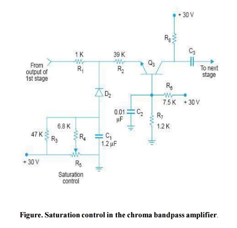
Manual Colour (Saturation) Control.
As shown in Fig. the chroma signal from the first stage is applied through R 1 and R 2 to the emitter of Q 3 and cathode of D 2 , the colour control diode. The diode is forward biased by a voltage divider formed by R 3 , R 4 and R 5 the colour control potentiometer.
When the diode is excessively forward biased (R 5 at + 30 V position) it behaves like a short circuit. Under this condition the chroma signal gets shorted via C 1 to ground and there is no input to the demodulators. As a result, a black and white picture is produced on the screen. If R 5 is so adjusted that forward bias on D 1 is almost zero, the diode would present a very high impedance to the signal.
Under this condition all the available signal feeds into the amplifier and a large signal voltage appears at the output of the chroma bandpass amplifier. This is turn produces a picture with maximum saturation.
At other settings of R 5 , conductance of D 1 would cause the signal current to divide between the emitter of Q 3 and C 1 resulting in intermediate levels of picture colour saturation.
No tint or hue control is provided in PAL receivers because of the inbuilt provision for phase shift cancellation. In same receiver designs the saturation control is combined with the contrast control.
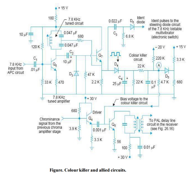
Colour Killer Circuit.
The colour killer and associated circuits are shown in Fig. The forward bias of Q 5 , the last stage of bandpass amplifier depends on the state of the colour killer circuit.
When a colour signal is being received, the 7.8 KHz (switching rate of the (R – Y) signal) component is available at the APC (automatic phase control) circuit of the reference subcarrier oscillator. It is applied via C 1 to the base of tuned amplifier Q 6 . The amplified 7.8 KHz signal is ac coupled to Q 7 .
Diode D 3 conducts on negative half cycles charges the capacitor C 2 with the polarity marked across it.
The discharge current from this capacitor provides forward bias to Q 7 , the emitter follower. Such an action results in a square wave signal at the output of Q 7 .
It is coupled back via a 680 ohm resistor to the tuned circuit in the collector of Q 6 . This provides positive feedback and thus improves the quality factor of the tuned circuit.
The colour killer diode D 4 rectifies the square-wave output from the emitter of Q 7 . The associated RC filter circuit provides a positive dc voltage at point ‘A’ and this serves a source of forward bias to the chrominance amplifier Q 5 . Diode D 5 is switched on by this bias and so clamps the voltage produced at ‘A’ by the potential divider (3.3 K and 680 ohm) across the + 15 V line.
When a monochrome transmission is received there is no 7.8 KHz input to the colour killer diode D 4 and no positive voltage is developed at its cathode (point A). Both D 5 and the base emitter junction of Q 5 are now back biased by the – 20 V potential returned at ‘A’ via the 220 K resistor.
The chrominance signal channel, therefore, remains interrupted.
(b) Separation of U and V modulation products.
The addition of two picture lines radiated in sequence but presented to the adder circuit simultaneously yields a signal consisting of only U information but with an amplitude equal to twice the amplitude of the chrominance signal’s U modulation product. Similarly the subtraction of the two lines produces a signal consisting of V information with an amplitude equal to twice that of the V modulation product.
Synchronous Demodulators.
The output from the adder and substractor consists of two independent double sideband, suppressed carrier RF signals. These are the U modulation product and the line-by-line phase inverted V modulation product. The two individual RF signals are fed to their respective demodulators.
Each of the demodulators also receives a controlled subcarrier of correct phase to allow recovery of the colour difference signal waveforms. It may be noted that the modulators do not have to handle Q.A.M. (u ± jv) RF signals as is the case in the NTSC system.
Therefore, it is not absolutely necessary to employ synchronous demodulators. However, synchronous demodulators are preferred in practice because they yield an accurate and constant no-colour zero voltage level above and below which (sometimes positive and sometimes negative) the colour different signal voltage varies. (c) Colour difference amplifiers and matrixing.
There are two approaches to driving the colour picture tube. In one scheme, the three colour difference signals are amplified and fed to the appropriate grids of the picture tube. The – Y signal is fed to the junction of three cathodes for matrixing. In another approach R, G, and B video signals are obtained directly by a suitable matrix from the modulator outputs. Each colour signal is then separately amplified and applied with negative polarity (– R, – G, – B) to the respective cathodes.
The grids are then returned to suitable negative dc potentials. This, i.e., R, G, B method is preferred in transistor amplifiers because less drive voltages are necessary when R, G, and B are directly fed to the picture tube.
The use of dc amplifiers would involve difficulties, especially in maintaining a constant ‘no colour’ voltage level at the picture tube grids. It is usual to employ ac amplifiers and then establish a constant no-colour level by employing dc clamps. The clamping is affected during line blanking periods by pulses derived from the line time base circuitry.
Thus the dc level is set at the beginning of each active line period. The discharge time constants of the ac coupling networks are chosen to be quite large so that the dc level does not change significantly between the beginning and end of one active line period.
6. Subcarrier Generation and Control
The primary purpose of this section is to produce a subcarrier of correct frequency to replace the subcarrier suppressed in the two chrominance signal balanced modulators at the transmitter end encoder. N ot only must the generated subcarrier be of exactly the right frequency but it must also be of the same phase reference as the original subcarrier. A crystal oscillator is used in the receiver and this is forced to work at the correct frequency and phase by the action of an automatic frequency and phase control circuit.
This is usually called the APC circuit. The APC circuit compares the burst and locally generated reference subcarrier to develop a control voltage. The burst signal is obtained through the burst gate amplifier circuit.
The identification circuit and electronic switch for line switching the subcarrier to the V modulator also form part of the subcarrier generation circuitry. (a) Burst gate amplifier. The burst gate or burst amplifier as it is often called separates
Related Topics