Chapter: Embedded and Real Time Systems : Computing Platform and Design Analysis
Memory Devices
MEMORY
DEVICES:
There are
several varieties of both read-only and read/write memories, each with its own
advantages. After discussing some basic characteristics of memories, we
describe RAMs and then ROMs.
1. Memory Device Organization
The most
basic way to characterize a memory is by its capacity, such as 256 MB. However,
manufacturers usually make several versions of a memory of a given size, each
with a different data width. For example, a 256-MB memory may be available in
two versions:
As a 64M *4-bit array, a single memory access
obtains an 8-bit data item, with a maximum of 226 different
addresses.
As a 32 M* 8-bit array, a single memory access
obtains a 1-bit data item, with a maximum of 223 different
addresses.
The
height/width ratio of a memory is known as its aspect ratio. The best
aspect ratio depends on the amount of memory required. Internally, the data are
stored in a two-dimensional array of memory cells as shown in Figure 2.4.
Because the array is stored in two dimensions, the n-bit address received by the chip is split into a row and a column
address (with n =r+ c).
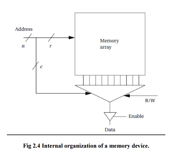
The row
and column select a particular memory cell. If the memory’s external width is 1
bit, the column address selects a single bit; for wider data widths, the column
address can be used to select a subset of the columns. Most memories include an
enable signal that controls the
tri-stating of data onto the memory’s pins.
2. Random-Access Memories:
Random-access memories can be both read and
written. They are called random access because, unlike magnetic disks,
addresses can be read in any order. Most bulk memory in modern systems is dynamic
RAM (DRAM). DRAM is very dense; it does, however, require that its
values be refreshed periodically
since the values inside the memory cells decay over time.
o The dominant form of dynamic RAM
today is the
synchronous
DRAMs (SDRAMs), which uses clocks to improve DRAM performance. SDRAMs use
Row Address Select (RAS) and Column Address Select (CAS) signals to break the
address into two parts, which select the proper row and column in the RAM
array. Signal transitions are relative to the SDRAM clock,which allows the
internal SDRAM operations to be pipelined.
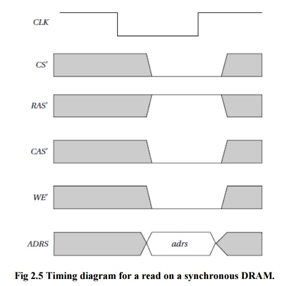
As shown
in Figure 2.5, transitions on the control signals are related to a clock
[Mic00]. RAS_ and CAS_ can therefore become valid at the same time.
The address lines are not shown in full detail
here; some address lines may not be active depending on the mode in use. SDRAMs
use a separate refresh signal to control refreshing. DRAM has to be refreshed
roughly once per millisecond.
Rather than refresh the entire memory at once,
DRAMs refresh part of the memory at a time. When a section of memory is being
refreshed, it cannot be accessed until the refresh is complete. The memory
refresh occurs over fairly few seconds so that each section is refreshed every
few microseconds.
SDRAMs include registers that control the mode in
which the SDRAM operates. SDRAMs support burst modes that allow several
sequential addresses to be accessed by sending only one address. SDRAMs
generally also support an interleaved mode that exchanges pairs of bytes.
3. Read-Only Memories:
Read-only memories (ROMs) are
preprogrammed with fixed data. They are very useful in embedded systems since a
great deal of the code, and perhaps some data, does not change over time.
Read-only memories are also less sensitive to radiation induced errors.
There are several varieties of ROM available. The
first-level distinction to be made is between factory-programmed ROM (sometimes
called mask-programmed ROM) and field-programmable ROM.
Factory-programmed ROMs are ordered from the
factory with particular programming. ROMs can typically be ordered in lots of a
few thousand, but clearly factory programming is useful only when the ROMs are
to be installed in some quantity.
Field-programmable ROMs, on the other hand, can be
programmed in the lab. Flash memory is the dominant form of
field-programmable ROM and is electrically erasable.
Flash memory uses standard system voltage for
erasing and programming, allowing it to be reprogrammed inside a typical
system. This allows applications such as automatic distribution of upgrades—the
flash memory can be reprogrammed while downloading the new memory contents from
a telephone line.
Early flash memories had to be erased in their
entirety; modern devices allow memory to be erased in blocks. Most flash
memories today allow certain blocks to be protected.
A common application is to keep the boot-up code in
a protected block but allow updates to other memory blocks on the device. As a
result, this form of flash is commonly known as boot-block flash.
Related Topics