Chapter: Electronic Devices and Circuits : Transistors
Important Short Questions and Answers: Transistors
TRANSISTORS
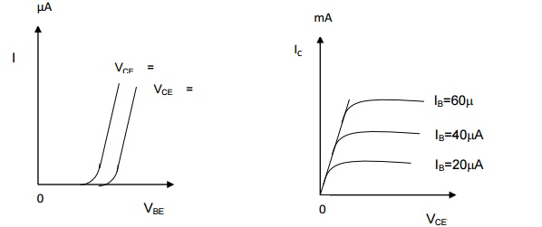
1. Draw
the input and output characteristics of a transistor in CE configuration and
mark the cutoff saturation and active regions.
2. State the advantage of optocouples?
·
Control
circuits are well protected due to electrical isolation.
·
Wideband
signal transmission is possible.
·
Due to
unidirected signal transfer , noise from the output side does not get coupled
to the input side.
·
Interfacing
with logic circuit is easily possible.
3. Why is
collector region wider than emitter region in BJT?
In BJT collector region is wider and base
region is thinner. The collector is made wider so as make heat dissipation
easier whereas thinner base will increase the value of β of the transistor.
4. In a
BJT,the emitter current is 12 mA and the emitter current is 1.02 times the
collector current. Find the base current.
IE= IC + IB =
1.02 IC (Given)
IB = 0.02 IC
But IC
= IE / 1.02
=
12/1.02
=
11.76 Ma
IB = 0.02 * 11.76 *10-3
=
235.2
µA.
5. Differentiate
FET and BJT ( two points)?
FET
Unipolar device (that is current conduction by
only one type of either electron or hole).
High input impedance due to reverse bias.
Gain is characterized by trans conductance
Low noise level
BJT
Bipolar device (current conduction by both
electron and hole).
Low input impedance due to forward bias.
Gain is characterized by voltage gain
High noise level
6.
Define pinch off voltage in FET.
The pinch off voltage VP is defined
as the value of VDS beyond which the drain current becomes constant.
7. Why
are power transistor provided with heat sinks?
To avoid thermal runway , which will damage the
transistor due to internal heating the power transistor provided with heat
sinks.
8. What are
the special features of FET
·
It is a
voltage controlled device.
·
It is
equivalent to a controlled current source.
·
The gate
source junction is always reverse biased.
·
Very
small gate current.
·
High
input resistance and input capacitance.
·
Can be
used as a switch or as an amplifier.
·
It can
be used as voltage variable resistance VVR.
9. Will a
transistor result if two diodes are connected back to back?
No, because
·
The
diode equivalent circuit cannot give the integrated effect of the transistor
and the base terminal has no control over the current flowing through the
diode.
·
The
reverse biased diode representing the collector junction will not allow the
current reverse to flow.
10.
Why FET is called unipolar device?
FET is a unipolar device, that means the
current flowing through it is only due to one type of charge particles, holes
or electrons . Transistor on the other hand is a bipolar device as holes and
electrons both contribute to the flow of current.
11. What
is a bipolar junction transistor?
A bipolar junction transistor is a three
terminal semiconductor deice in which the operation depends on the interaction
of both majority and minority carriers.
12.
Define the different operating regions of
transistor.
The different operating regions of transistor
are
Active
Region: It is defined in which
transistor function is biased in reverse direction
and emitter function in forward direction.
Cutoff
Region: The region
in which the collector and emitter functions are both reverse biased.
Saturation
Region: The region
in which both the collector and emitter functions are forward biased.
13.
Explaip npn and pnp transistor.
npn
Transistor: In
npn transistor, P-type semiconductor is sandwiched between two n-type
semiconductors. The emitter region is made up of n-type semiconductor base
region is made of p-type semiconductor, collector region is made of n-type
semiconductor.
pnp
Transistor: In
pnp transistor, n-type semiconductor is sandwiched between two P-type semiconductor. Emitter region
is made of P-type, collector region is made of P-type and the base region is
made of n-type, semiconductor.
14.
Define Transistor current.
The emitter current (1E) is the sum
of the collector current (Ic) and the base current (IB), is called transistor
current'. IE = Ic + IB;. IB is very small compared to IE or Ic.
15.
What are the three types of configuration in transistors?
Depending on the input, output and
.common terminal a transistor are connected in 3 configurations;
i) Common base configuration
ii) Common emitter configuration
iii) Common collector-Configuration.
16.
What is early effect or base and the modulation?
As the collector by voltage Vcc is
made to increase the reverse bias, the space charge width between collector and
base tends to increase with the result that the effective width of the base
decreases. This dependency of base width on collector to emitter -voltage is
known as early effect.
Related Topics