Chapter: Electronic Devices and Circuits : Transistors
Field Effect Transistor(FET) and its Operation
Field Effect Transistor:
The field effect transistor is a semiconductor device, which depends for its operation on the control of current by an electric field. There are two of field effect transistors:
1. JFET (Junction Field Effect Transistor)
MOSFET (Metal Oxide Semiconductor Field Effect Transistor)
The FET has several advantages over conventional transistor.
1. In a conventional transistor, the operation depends upon the flow of majority and minority carriers. That is why it is called bipolar transistor. In FET the operation depends upon the flow of majority carriers only. It is called unipolar device.
2. The input to conventional transistor amplifier involves a forward biased PN junction with its inherently low dynamic impedance. The input to FET involves a reverse biased PN junction hence the high input impedance of the order of M-ohm.
3. It is less noisy than a bipolar transistor.
4. It exhibits no offset voltage at zero drain current.
5. It has thermal stability.
6. It is relatively immune to radiation.
The main disadvantage is its relatively small gain bandwidth product in comparison with conventional transistor.
1. Operation of FET:
Consider a sample bar of N-type semiconductor. This is called N-channel and it is electrically equivalent to a resistance as shown in fig. 1.
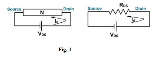
Ohmic contacts are then added on each side of the channel to bring the external connection. Thus if a voltage is applied across the bar, the current flows through the channel.
The terminal from where the majority carriers (electrons) enter the channel is called source designated by S. The terminal through which majority carriers leaves the channel is called drain and designated by D. For an N-channel device, electrons are the majority carriers. Hence the circuit behaves like a dc voltage VDS applied across a resistance RDS. The resulting current is the drain current ID. If VDS increases, ID increases proportionally.
Now on both sides of the n-type bar heavily doped regions of p-type impurity have been formed by any method for creating pn junction. These impurity regions are called gates (gate1 and gate2) as shown in fig. 2.
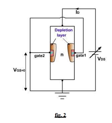
Both the gates are internally connected and they are grounded yielding zero gate source voltage (VGS =0). The word gate is used because the potential applied between gate and source controls the channel width and hence the current.
As with all PN junctions, a depletion region is formed on the two sides of the reverse biased PN junction. The current carriers have diffused across the junction, leaving only uncovered positive ions on the n side and negative ions on the p side. The depletion region width increases with the magnitude of reverse bias. The conductivity of this channel is normally zero because of the unavailability of current carriers.
The potential at any point along the channel depends on the distance of that point from the drain, points close to the drain are at a higher positive potential, relative to ground, then points close to the source. Both depletion regions are therefore subject to greater reverse voltage near the drain. Therefore the depletion region width increases as we move towards drain. The flow of electrons from source to drain is now restricted to the narrow channel between the no conducting depletion regions. The width of this channel determines the resistance between drain and source.
Consider now the behavior of drain current ID vs drain source voltage VDS. The gate source voltage is zero therefore VGS= 0. Suppose that VDS is gradually linearly increased linearly from 0V. ID also increases.
Since the channel behaves as a semiconductor resistance, therefore it follows ohm's law. The region is called ohmic region, with increasing current, the ohmic voltage drop between the source and the channel region reverse biased the junction, the conducting portion of the channel begins to constrict and ID begins to level off until a specific value of VDS is reached, called the pinch of voltage VP.
At this point further increase in VDS do not produce corresponding increase in ID. Instead, as VDS increases, both depletion regions extend further into the channel, resulting in a no more cross section, and hence a higher channel resistance. Thus even though, there is more voltage, the resistance is also greater and the current remains relatively constant. This is called pinch off or saturation region. The current in this region is maximum current that FET can produce and designated by IDSS. (Drain to source current with gate shorted)
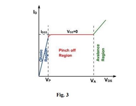
As with all pn junctions, when the reverse voltage exceeds a certain level, avalanche breakdown of pn junction occurs and ID rises very rapidly as shown in fig. 3.
Consider now an N-channel JFET with a reverse gate source voltage as shown in fig. 4.
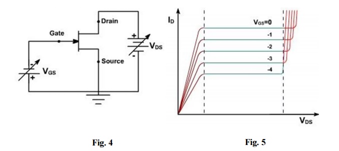
The additional reverse bias, pinch off will occur for smaller values of | VDS |, and the maximum drain current will be smaller. A family of curves for different values of VGS(negative) is shown in
fig. 5.
Suppose that VGS= 0 and that due of VDS at a specific point along the channel is +5V with respect toground. Therefore reverse voltage across either p-n junction is now 5V. If VGS is decreased from 0 to –1V the net reverse bias near the point is 5 - (-1) = 6V. Thus for any fixed value of VDS, the channel width decreases as VGS is made more negative.
Thus ID value changes correspondingly. When the gate voltage is negative enough, the depletion layers touch each other and the conducting channel pinches off (disappears). In this case the drain current is cut off. The gate voltage that produces cut off is symbolized VGS(off) . It is same as pinch off voltage.
Since the gate source junction is a reverse biased silicon diode, only a very small reverse current flows through it. Ideally gate current is zero. As a result, all the free electrons from the source go to the draini.e. ID = IS. Because the gate draws almost negligible reverse current the input resistance is very high 10's or 100's of M ohm. Therefore where high input impedance is required, JFET is preferred over BJT. The disadvantage is less control over output current i.e. FET takes larger changes in input voltage to produce changes in output current. For this reason, JFET has less voltage gain than a bipolar amplifier.
Transductance Curves:
The transductance curve of a JFET is a graph of output current (ID) vs input voltage (VGS) as shown in fig. 1.
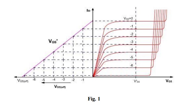
By reading the value of ID and VGS for a particular value of VDS, the transductance curve can be plotted. The transductance curve is a part of parabola. It has an equation of
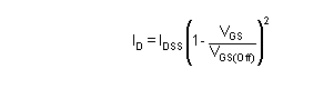
Data sheet provides only IDSS and VGS(off) value. Using these values the transductance curve can be plotted.
Related Topics