Chapter: Electronic Devices and Circuits : Transistors
Transistors: Types, Construction, Currents
TRANSISTORS
INTRODUCTION
The transistor is the main building block ―element‖ of electronics. It is a semiconductor device and it comes in two general types: the Bipolar Junction Transistor (BJT) and the Field Effect Transistor (FET).
It is named as transistor which is an acronym of two terms: ―transfer-of-resistor.‖ It means that the internal resistance of transistor transfers from one value to another values depending on the biasing voltage applied to the transistor. Thus it is called Transfer resistor: i.e.
TRANSISTOR.
A bipolar transistor (BJT) is a three terminal semiconductor device in which the operation depends on the interaction of both majority and minority carriers and hence the name bipolar.
The voltage between two terminals controls the current through the third terminal. So it is called current controlled device. This is the basic principle of the BJT
It can be used as amplifier and logic switches. BJT consists of three terminals:
Collector : C
Base : B
Emitter : E
Ø TYPES
There are two types of bipolar transistors
NPN transistor and
PNP transistor.
1. TRANSISTOR CONSTRUCTION
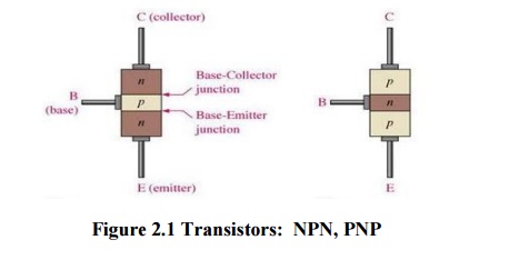
PNP Transistor: In PNP transistor a thin layer of N-type silicon is sandwiched between two layers of P-type silicon.
NPN Transistor: In NPN transistor a thin layer of P-type silicon is sandwiched between two layers of N-type silicon. The two types of BJT are represented in figure 2.1
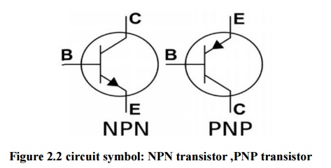
The symbolic representation of the two types of the BJT is shown in figure 2.2
Area:[C>E>B]
The area of collector layer is largest. So it can dissipate heat quickly.
Area of base layer is smallest and it is very thin layer.
Area of emitter layer is medium.
Doping level:[E>C>B]
Collector layer is moderately doped. So it has medium number of charges.
Base layer is lightly doped. So it has a very few number of charges.
Emitter layer is heavily doped. So it has largest number of charges.
Junctions:
There are two junctions in this transistor – junction J-1 and junction J-2.
The junction between collector layer and base layer is called as collector-base junction or C-B junction.
The junction between base layer and emitter layer is called as base-emitter junction or B-E junction. The two junctions have almost same potential barrier voltage of 0.6V to 0.7V, just like in a diode.
Equivalent diode representation:
The transistor formed by back to back connection of two diodes
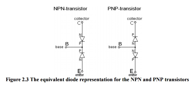
The states of the two pn junctions can be altered by the external circuitry connected to the transistor. This is called biasing the transistor.
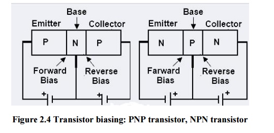
Usually the emitter- base junction is forward biased and collector –base junction is reverse biased. Due to forward bias on the emitter- base junction an emitter current flows through the base into the collector. Though, the collector –base junction is reverse biased, almost the entire emitter current flows through the collector circuit.
A single pn junction has two different types of bias:
· Forward bias
· Reverse bias
There are two junctions in bipolar junction transistor. Each junction can be forward or reverse biased independently. Thus there are four modes of operations:
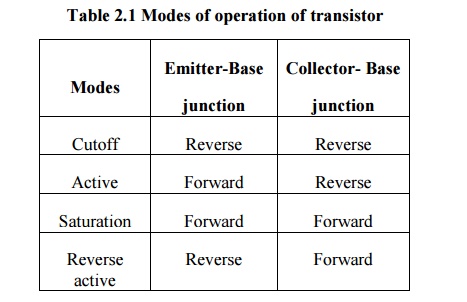
Forward Active
In this mode of operation, emitter-base junction is forward biased and collector base junction is reverse biased. Transistor behaves as a source. With controlled source characteristics the BJT can be used as an amplifier and in analog circuits.
Cut off
When both junctions are reverse biased it is called cut off mode. In this situation there is nearly zero current and transistor behaves as an open switch.
Saturation
In saturation mode both junctions are forward biased large collector current flows with a small voltage across collector base junction. Transistor behaves as an closed switch.
Reverse Active
It is opposite to forward active mode because in this emitter base junction is reverse biased and collector base junction is forward biased. It is called inverted mode. It is no suitable for amplification.However the reverse active mode has application in digital circuits and certain analog switching circuits.
2. TRANSISTOR CURRENTS
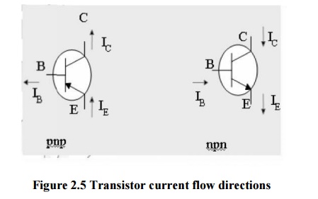
- The arrow is always drawn on the emitter The arrow always point toward the n-type
- The arrow indicates the direction of the emitter current:
pnp:E-> B
npn: B-> E
IC = the collector current, IB = the base current, IE = the emitter current
Related Topics