Chapter: Electronic Devices and Circuits : PN Junction Devices
Important Short Questions and Answers: PN Junction Devices
PN JUNCTION DEVICES
1.What
is a PN Junction ?How is it formed?
In a piece of semiconductor material if one
half is doped by P-type impurity and other half is doped by N-type impurity, a
PN Junction diode is formed. The plane dividing the two halves (or) zones is
called PN Junction.
2. What
is meant by diffusion capacitance (CD)?
The capacitance that exists in a forward bias
junction is called a diffusion (or) storage capacitance (Cp) whose value is
usually much larger than Cr, which exists in reverse based junction. This also
defined as the rate of change of injected charge with applied voltage
Cp = (dQ/dW),
where
dQ -» represents the change in the number of
minority carriers stored outside the depletion region when a change in voltage
across the diode,
dv is applied.
3.What
is Zener diode?
Zener diode is a specially designed PN junction
diode. A reverse biased heavily doped PN junction diode. A reverse biased
heavily doped PN junction diode which is operated in the breakdown region is
known as Zener diode. It is also called as voltage regulator diode or breakdown
diode.
4. List out
the applications of LED.
·
LEDs are
more popularly used in display clocks , audio
and video equipments ,traffic lights.
·
It is
also used as light source in optical fibre communication.
5. Define
transition capacitance of P-N diode.
When a diode is reverse biased , the holes in
the p- side and the electrons in the n-side drift away from the junction ,
thereby uncovering more immobile charges. As a result the thickness of
depletion increases . this leads to capacitance effect across the region called
transition capacitance.
6.
Distinguish between shunt and series voltage regulator.
·
Series
regulator
In a series regulator the regulating element is
in series with the load and the regulation is done by varying the voltage
across the series element.
·
Shunt
regulator
In a shunt regulator the regulating element is
in shunt with the load and the regulation is done by varying the current across
the shunt element.
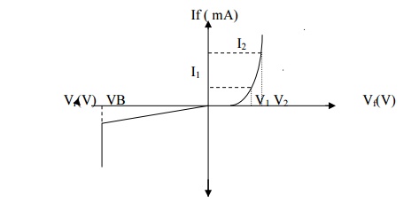
7. Draw
the VI Characteristics of Zener diode.
8.
Derive the ripple factor of full wave rectifier.
The ripple factor is a measure of how
successfully a rectifier converts ac to dc. That is it is the ratio of rms
value of ac component to the dc value.
Ripple factor= Vr(rms)/Vdc
9.
Define peak inverse voltage in a diode.
Peak inverse voltage is the maximum negative
voltage which appears across a non conducting reverse biased voltage.
10. What
is Drift Current?
Under the influence of the externally applied
electric field , the electrons are accelerated in one particular direction.
They travel at a speed equal to drift speed. This movement of electrons will
give rise to a current which is defined as the drift current.
11. What
is barrier potential at the junction?
Due to the presence of immobile positive and
negative ions on opposite sides of the junction an electric field is created
across the junction . The electric field is known as the barrier potential.
12.What
is a Rectifier?
A rectifier is a device which converts a.c.
voltage to pulsating d.c. voltage, using one or more
Pn junction diodes. Its types
i)half wave rectifier
ii)full wave rectifier
13. What
is meant by drift current?
When an electric field is applied across the
semiconductor material, the charge carriers attain a certain drift velocity
which is equal to the product of the mobility of the charge carriers and the
applied electric field intensity E. The holes move towards the negative
terminal of the battery and electron move towards the positive terminal. This
combined effect of movement of the charge carriers constitute a current known
as drift current.
14.
Define Hall effect?
If a metal or semiconductor carrying current I
is placed in a transverse magnetic field B , an electric field E is induced in
the direction perpendicular to both I and B , This phenomenon is known as Hall
effect.
15.Give
some application of Hall Effect.
i. hall effect can be used to measure the strength
of a magnetic field in terms of electrical voltage.
ii. it is used to determine whether the
semiconductor is p – type or n- type material
iii. it is used to determine the carrier
concentration
iv.it is used to determine the mobility.
Related Topics