Chapter: Electronic Circuits : BJT Amplifiers
Midband analysis of BJT Single Stage Amplifiers
Midband analysis of BJT Single
Stage Amplifiers:
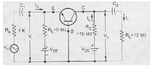
Consider
the basic amplifier circuit. To form a transistor amplifier only is is
necessary to connect an external load and signal source along with proper
biasing.
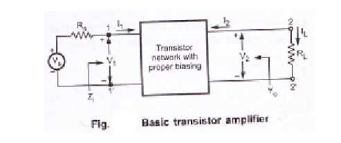
We can
replace the transistor circuit as shown in the following figure.
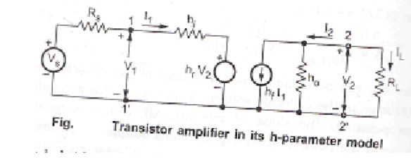
Let us
analyze the hybrid model to find current gain, input resistance, voltage gain
and output resistance.
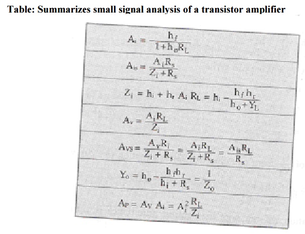
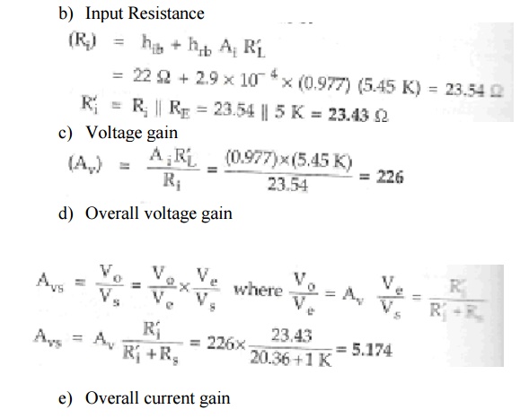
Current gain (Ai):
It is
defined as the ratio of output to input current. It is given by,

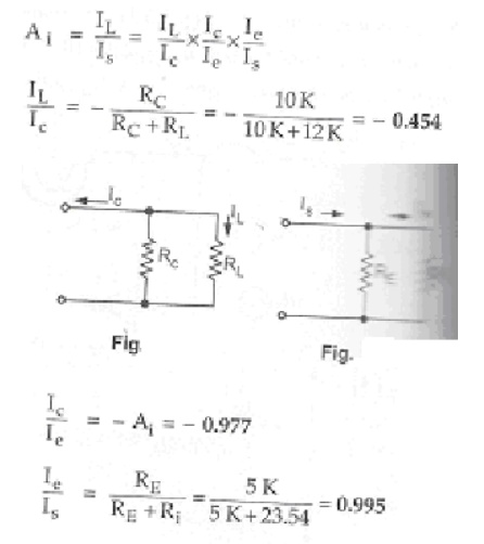
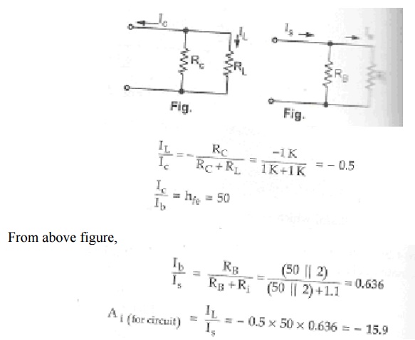
Here IL
and I2 are equal in magnitude but opposite in sign. IL =
-I2
From
above circuit
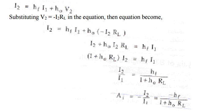
It is given by,
From above figure, using current divider rule,

Input Impedance (Zi):
Ri
is the input resistance looking into the amplifier input terminals ( 1, 1’). It
is given by,

From the
input circuit,
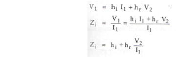
Substituting V2 = -I2RL = Ai I1 RL in the above equation,
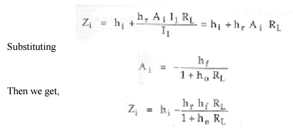
Dividing
numerator and denominator by RL we get,
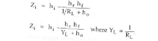
From this
equation, note that the input impedance is a function offload impedance.
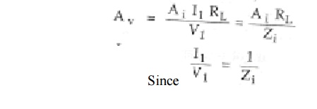
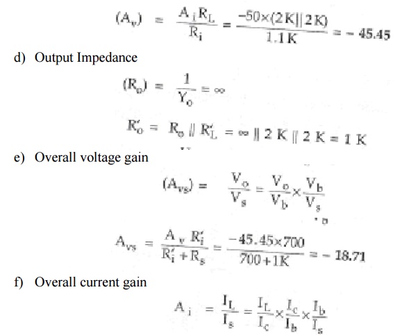
Voltage gain (Av):
It is the
ratio of output voltage to input voltage. It is given by,

By
substituting V2 = -I2RL = Ai I1
RL
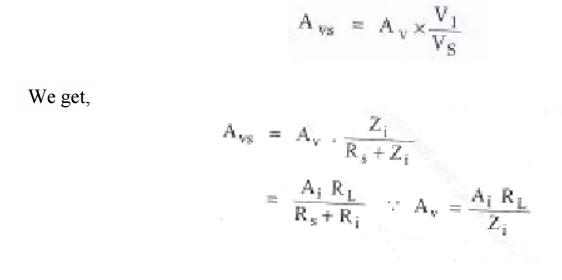
Voltage gain (Avs):
It is
voltage gain including the source. It is given by,

From
above figure, applying potential divider rule, then we get,
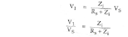
Substituting
the value of V1/Vs in the equation of
Output Admittance (Yo):
It is the
ratio of output current to output voltage. It is given by,
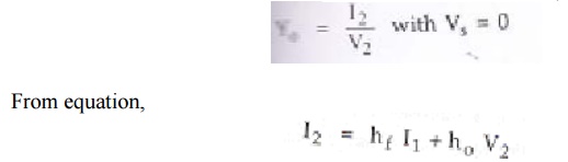
Dividing
above equation by V2, We get,

From
transistor amplifier in h-parameter model circuit, with Vs = 0,
RsI1 + hiI1 +hrV2 = 0
(Rs + hi)
I 1 = -hr V2
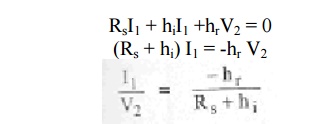
Substituting
the value of I1/V2 from above equation in the equation of
Yo. We obtain,

From this
equation, note that the output admittance is a function of source resistance.
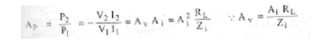
Power gain (Ap):
It is the
ratio of average power delivered to the load to the input power. Output power
is given as,

Since the
input power is P1 = V1I1
The
operating power gain Ap of the transistor is given as,
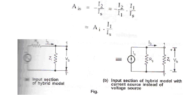
Relation between Avs and AIS
From
equation,
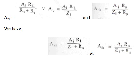
Taking
ratio of above two equations we get,

Method for analysis of a transistor circuit:
The
analysis of transistor circuits for small signal behaviour can be made by
following simple guidelines. These guidelines are,
1. Draw the
actual circuit diagram
2. Replace
coupling capacitors and emitter bypass capacitor by short circuit
3. Replace
D.C. source by a short circuit
4. Mark the
points B, E, C on the circuit diagram and locate these points as the start of
the equivalent circuit
5. Replace
the transistor by its h-parameter model
Problem 1:
For the
common base circuit shown in figure, transistor parameters are hib =
22Ω,
hfb
= -0.98, hob = 0.49µA/V, hrb = 2.9*10 -4.
Calculate the values of input resistance, output resistance, current gain and
voltage gain for the given circuit.
Solution:
Change
the given figure into h-parameter equivalent model.
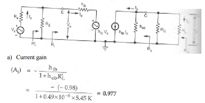
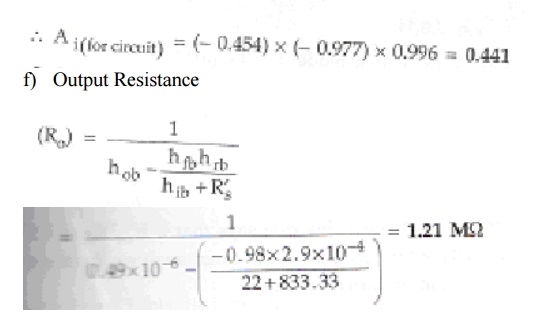
Ro'
= Ro || RL’ = 1.21M || 5.45K = 5.425KΩ
Problem 2:
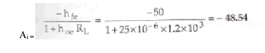
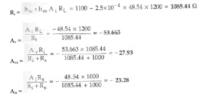
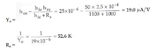
Consider
a single stage CE amplifier with Rs = 1KΩ, RL = 1.2KΩ. Calculate Ai,
Ri, Av, Ais,
power gain and Ro if hie = 1.1k, hre = 2.5*10-4,
hfe = 50 and hoe = 25µA/V.
Solution:
Problem 3:
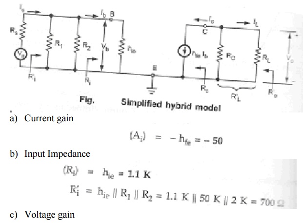
Consider
a single stage CE amplifier with Rs = 1k, R1 = 50k, R2
= 2k, Rc = 2k, RL =
2K, hie = 1.1k, hoe = 25µA/V, hfe = 50
and hre = 2.5*10-4 as shown in the figure.
Find Ai,
Ri, Av, Ai, Avs and Ro.
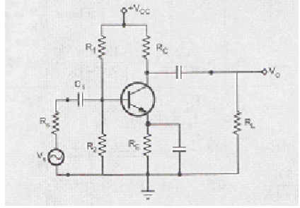
Solution:
Since hoe
RL' = 25*10-6*(2K || 2K) = 0.25, which is less than 0.1, so use
approximate analysis.
Consider
the simplified hybrid model for the given circuit.
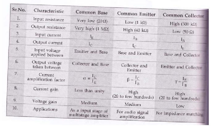
Comparison of Transistor Configurations:
Related Topics