Chapter: Microprocessor and Microcontroller : I/O Interfacing
8279 Programmable Keyboard/Display Controller
8279 Programmable Keyboard/Display Controller
Intel’s
8279 is a general purpose Keyboard Display controller that simultaneously
drives the display of a system and interfaces a Keyboard with the CPU. The
Keyboard Display interface scans the Keyboard to identify if any key has been
pressed and sends the code of the pressed key to the CPU. It also transmits the
data received from the CPU, to the display device.
Both of these functions are performed by the
controller in repetitive fashion without involving the CPU. The Keyboard is
interfaced either in the interrupt or the polled mode. In the interrupt mode,
the processor is requested service only if any key is pressed, otherwise the
CPU can proceed with its main task.
In the polled mode, the CPU periodically reads an
internal flag of 8279 to check for a key pressure. The Keyboard section can
interface an array of a maximum of 64 keys with the CPU. The Keyboard entries
(key codes) are debounced and stored in an 8-byte FIFO RAM, that is further
accessed by the CPU to read the key codes. If more than eight characters are
entered in the FIFO (i.e. more that eight keys are pressed), before any FIFO
read operation, the overrun status is set. If a FIFO contains a valid key
entry, the CPU is interrupted (in interrupt mode) or the CPU checks the status
(in polling) to read the entry.
Once the
CPU reads a key entry, the FIFO is updated, i.e. the key entry is pushed out of
the FIFO to generate space for new entries. The 8279 normally provides a
maximum of sixteen 7-seg display interface with CPU It contains a 16-byte
display RAM that can be used either as an integrated block of 16x8-bits or two
16x4-bit block of RAM. The data entry to RAM block is controlled by CPU using
the command words of the 8279.
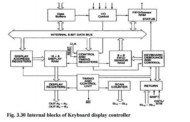
ü Architecture and Signal Descriptions of 8279
The
Keyboard display controller chip 8279 provides
1. A set of
four scan lines and eight return lines for interfacing keyboards.
2. A set of
eight output lines for interfacing display.
ü I/O Control and Data Buffer
The I/O
control section controls the flow of data to/from the 8279. The data buffer
interface the external bus of the system with internal bus of 8279 the I/O
section is enabled only if D is low.
The pin Ao, RD and WR select the command, status
or data read/write operations carried out by the CPU with 8279.
ü Control
and Timing Register and Timing Control
These
registers store the keyboard and display modes and other operating conditions
programmed by CPU. The registers are written with Ao=1 and WR =0. The timing and control unit controls the basic
timings for the operation of the circuit. Scan Counter divide down the
operating frequency of 8279 to derive scan keyboard and scan display
frequencies.
ü Scan
Counter
The Scan
Counter has two modes to scan the key matrix and refresh the display. In the
Encoded mode, the counter provides a binary count that is to be externally
decoded to provide the scan lines for keyboard and display (four externally decoded
scan lines may drive up to 16 displays). In the decoded scan mode, the counter
internally decodes the least significant 2 bits and provides a decoded 1 out of
4 scan on SL0-SL3 (four internally decoded scan lines may drive up to 4 Displays).
The Keyboard and Display both are in the same mode at a time.
Return Buffers and Keyboard Debounce and Control
This
section scans for a Key closure row-wise. If it is detected, the Keyboard
debounce unit debounces the key entry (i.e. wait for 10 ms). After the debounce
period, if the key continues to be detected. The code of the Key is directly
transferred to the sensor RAM along with SHIFT and CONTROL key status.
FIFO/Sensor RAM and Status Logic
In
Keyboard or strobed input mode, this block acts as 8-byte first-in-first-out
(FIFO) RAM. Each key code of the pressed key is entered in the order of the
entry, and in the meantime, read by the CPU, till the RAM becomes empty. The
status logic generates an interrupt request after each FIFO read operation till
the FIFO is empty.
In
scanned sensor matrix mode, this unit acts as sensor RAM. Each row of the
sensor RAM is loaded with the status of the corresponding row of sensors in the
matrix. If a sensor changes its state, the IRQ line goes high to interrupt the
CPU.
Display Address Registers and Display RAM.
The
Display address registers hold the addresses of the word currently being
written or read by the CPU to or from the display RAM. The contents of the
registers are automatically updated by 8279 to accept the next data entry by
CPU. The 16-byte display RAM contains the 16-byte of data to be displayed on
the sixteen 7-seg displays in the encoded scan mode.
ü Pin
Diagram of 8279
DB0 - DB7:
These are
bidirectional data bus lines. The data and command words to and from the CPU
are transferred on these lines.
CLK:
This is a
clock input used to generate internal timings required by 8279.
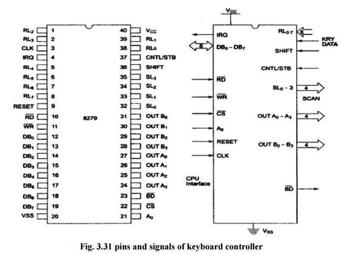
RESET:
This pin
is used to reset 8279. A high on this line resets 8279. After resetting 8279,
its in sixteen 8-bit display, left entry encoded scan, 2-key lock out mode. The
clock prescaler is set to 31.
CS chip select:
A low on
this line enables 8279 for normal read or write operations. Otherwise this pin
should be high.
Ao:
A high on
the Ao line indicates the transfer
of a command or status information. A low on this line indicates the transfer
of data. This is used to select one of the internal registers of 8279.
RD, WR:
(Input/Output)
READ/WRITE input pins enable the data buffer to receive or send data over the
data bus.
IRQ:
This
interrupt output line goes high when there is data in the FIFO sensor RAM. The
interrupt line goes low with each FIFO RAM read operation. However, if the FIFO
RAM further contains any Key-code entry to be read by the CPU, this pin again
goes high to generate an interrupt to the CPU.
Vss, Vcc:
These are
the ground and power supply lines for the circuit.
SL0-SL3 – Scan Lines:
These
lines are used to scan the keyboard matrix and display digits. These lines can
be programmed as encoded or decoded, using the mode control register.
RL0-RL7 – Return Lines:
These are
the input lines which are connected to one terminal of keys, while the other
terminal of the keys are connected to the decoded scan lines. These are
normally high, but pulled low when a key is pressed.
SHIFT:
The
status of the Shift input line is stored along with each key code in FIFO in
the scanned keyboard mode. Till it is pulled low with a key closure it is
pulled up internally to keep it high.
CNTL/STB-CONTROL/STROBED I/P Mode:
In the
Keyboard mode, this line is used as a control input and stored in FIFO on a key
closure. The line is a strobe line that enters the data into FIFO RAM, in the
strobed input mode. It has an internal pull up. The line is pulled down with a
Key closure.
BD – Blank Display:
This
output pin is used to blank the display during digit switching or by a blanking
command.
OUTA0 – OUTA3 and OUTB0 – OUTB3:
These are
the output ports for two 16x4 (or one 16 x 8) internal display refresh
registers. The data from these lines is synchronized with the scan lines to
scan the display and keyboard. The two 4-bit ports may also be used as one
8-bit port.
Modes of Operation of 8279
The Modes
of operation of 8279 are
i. Input
(Keyboard) modes
ii. Output
(Display) modes
Input (Keyboard) modes:
8279
provides three input modes, they are:
1. Scanned Keyboard Mode:
This mode
allows a key matrix to be interfaced using either encoded or decoded scans. In
the encoded scan, an 8 x 8 keyboard or in decoded scan , a 4 x 8 Keyboard can
be interfaced. The code of key pressed with SHIFT and CONTROL status is stored
into the
FIFO RAM.
2. Scanned Sensor Matrix:
In this
mode, a sensor array can be interfaced with 8279 using either encoder or
decoder scans. With encoder scan 8 x 8 sensor matrix or with decoder scan 4 x 8
sensor matrix can be interfaced. The sensor codes are stored in the CPU
addressable sensor RAM.
3. Strobed Input:
In this
mode, if the control line goes low, the data on return lines, is stored in the
FIFO byte by byte.
Output (Display) Modes:
8279
provides two output modes for selecting the display options.
1. Display Scan:
In this
mode, 8279 provides 8 or 16 character multiplexed displays those can be
organized as dual 4-bit or single 8-bit display units.
2. Display Entry:
The
Display data is entered for display either from the right side or from the left
side.
Details of Modes of Operation Keyboard Modes
1. Scanned Keyboard Mode with 2 Key Lockout
In this
mode of operation, when a key is pressed, a debounce logic comes into
operation. The Key code of the identified key is entered into the FIFO with
SHIFT and CNTL status, provided the FIFO is not full.
2. Scanned Keyboard with N-key Rollover
In this
mode, each key depression is treated independently. When a key is pressed, the
debounce circuit waits for 2 keyboard scans and then checks whether the key is
still depressed. If it is still depressed, the code is entered in FIFO RAM. Any
number of keys can be pressed simultaneously and recognized in the order, the
Keyboard scan record them.
3. Scanned Keyboard Special Error Mode
This mode
is valid only under the N-Key rollover mode. This mode is programmed using end interrupt/error mode set command. If
during a single debounce period (two Keyboard scan) two keys are found pressed, this is considered a
simultaneous depression and an error flag is set. This flag, if set, prevents
further writing in FIFO but allows generation of further interrupts to the CPU
for FIFO read.
3. Sensor Matrix Mode
In the
Sensor Matrix mode, the debounce logic is inhibited the 8-byte memory matrix.
The status of the sensor switch matrix is fed directly to sensor RAM matrix
Thus the sensor RAM bits contains the row-wise and column-wise status of the
sensors in the sensor matrix. 8
Display Modes
There are
various options of data display The first one is known as left entry mode or
type writer mode. Since in a type writer the first character typed appears at
the left-most position, while the subsequent characters appears successively to
the right of the first one. The other display format is known as right entry
mode, or calculator mode, since the calculator the first character entered
appears to the right-most position and this character is shifted one position
left when the next character is entered.
1. Left Entry Mode
In the
Left entry mode, the data is entered from the left side of the display unit.
Address 0 of the display RAM contains the leftmost display character and
address 15 of the RAM contains the rightmost display character.
2. Right Entry Mode
In the
right entry mode, the first entry to be displayed is entered on the rightmost
display. The next entry is also placed in the right most display but after the
previous display is shifted left by one display position.
ü Command
Words of 8279
All the
Command words or status words are written or read with Ao = 1 and CS = 0 to or
from 8279.
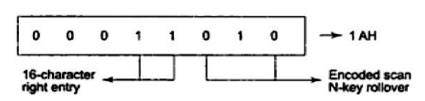
a. Keyboard Display mode set
The
format of the command word to select different modes of operation of 8279 is
given below with its bit definitions.
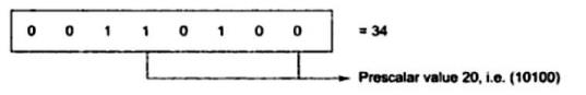
b. Programmable Clock
The clock
for operation of 8279 is obtained by dividing the external clock input signal
by a programmable constant called prescaler.
PPPPP is
a 5-bit binary constant. The input frequency is divided by a decimal constant
ranging from 2 to 31, decided by the bits of an internal prescalar, PPPPP.
c. Read FIFO/Sensor RAM
The format of this command is given as shown below X - don’t care
AI - Auto
increment flag
AAA -
Address pointer to 8 bit FIFO RAM
This word
is written to set up 8279 for reading FIFO/Sensor RAM. In scanned keyboard
mode, AI and AAA bits are of no use. The 8279 will automatically drive data bus
for each subsequent read, in the same sequence, in which the data was entered.
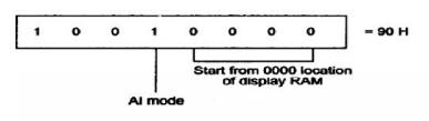
d. Read Display RAM
This command
enables a programmer to read the display RAM data The CPU writes this command
word to 8279 to prepare it for display RAM read operation. AI is auto
incremented flag and AAAA, the 4-bit address, points to the 16-byte display RAM
that is to be read. If AI = 1, the address will be automatically, incremented
after each read or write to the display RAM.
e. Write Display RAM
The
format of this command is given as shown below
AI - Auto
increment flag
AAAA -
4-bit address for 16-bit display RAM to be written
Other
details of this command are similar to the ‘Read Display RAM Command.
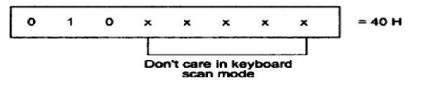
f. Display Write Inhibit/Blanking
The IW
(Inhibit write flag) bits are used to mask the individual nibble Here Do and D2
corresponds to OUTBo – OUTB3 while D1
and D3 corresponds to OUTAo-OUTA3
for blanking and masking respectively.
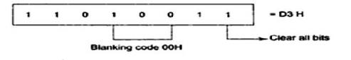
g. Clear Display RAM
The CD2, CD1, CDo is a selectable blanking code to clear all the rows of the
display RAM as given below. The characters A and B represents the output
nibbles.
CD CD1 CDo
1 0 x All
Zeros (x don’t care) AB = 00
1 1 0 A3-Ao = 2(0010) and B3-Bo = 00(0000) 1 1 1 All ones (AB =
FF), i.e. clear RAM
Here, CA
represents clear All and CF represents Clear FIFO RAM
End Interrupt/Error Mode Set
For the
sensor matrix mode, this command lowers the IRQ line and enables further
writing into the RAM. Otherwise, if a charge in sensor value is detected, IRQ
goes high that inhibits writing in the sensor RAM.
Key-code and status Data Formats
This
briefly describes the formats of the Key-code/Sensor data in their respective
modes of operation and the FIFO Status Word formats of 8279.
Key-code Data Formats:
After a
valid Key closure, the key code is entered as a byte code into the FIFO RAM, in
the following format, in scanned keyboard mode. The Keycode format contains
3-bit contents of the internal row counter, 3-bit contents of the column
counter and status of the SHIFT and CNTL Keys The data format of the Keycode in
scanned keyboard mode is given below. In the sensor matrix mode, the data from the
return lines is directly entered into an appropriate row of sensor RAM, that
identifies the row of the sensor that changes its status. The SHIFT and CNTL
Keys are ignored in this mode. RL bits represent the return lines.
Rn
represents the sensor RAM row number that is equal to the row number of the
sensor array in which the status change was detected. Data Format of the sensor
code in sensor matrix mode
FIFO Status Word:
The FIFO
status word is used in keyboard and strobed input mode to indicate the error.
Overrun error occurs, when an already full FIFO is attempted an entry, Under
run error occurs when an empty FIFO read is attempted. FIFO status word also
has a bit to show the unavailability of FIFO RAM because of the ongoing
clearing operation.
In sensor
matrix mode, a bit is reserved to show that at least one sensor closure
indication is stored in the RAM, The S/E bit shows the simultaneous multiple
closure error in special error mode. In sensor matrix mode, a bit is reserved
to show that at least one sensor closure indication is stored in the RAM, The
S/E bit shows the simultaneous multiple closure error in special error mode.
Interfacing and Programming 8279
Problem:
Interface
keyboard and display controller 8279 with 8086 at address 0080H. Write an ALP
to set up 8279 in scanned keyboard mode with encoded scan, N-Key rollover mode.
Use a 16
character display in right entry display format. Then clear the display RAM
with zeros. Read the FIFO for key closure. If any key is closed, store it’s
code to register CL.
Then
write the byte 55 to all the displays, and return to DOS. The clock input to
8279 is 2MHz, operate it at 100KHz.
Solution:
_ The
8279 is interfaced with lower byte of the data bus, i.e. Do-D7 . Hence the Ao input of 8279 is
connected with address lineA1.
_ The
data register of 8279 is to be addressed as 0080H, i.e.Ao=0.
_ For
addressing the command or status word Ao input of 8279 should be 1. _ The next
step is to write all the required command words for this problem.
Keyboard/Display Mode Set CW:
This
command byte sets the 8279 in 16-character right entry and encoded scan N-Key
rollover mode.
Program clock selection:
The clock
input to 8279 is 2MHz, but the operating frequency is to be 100KHz, i.e. the
clock input is to be divided by 20 (10100). Thus the prescalar value is 10100
and trhe command byte is set as given.
Clear Display RAM:
This
command clears the display RAM with the programmable blanking code.
Read FIFO:
This
command byte enables the programmer to read a key code from the FIFO RAM
Write Display RAM:
This
command enables the programmer to write the addressed display locations of the
RAM as presented below.
Related Topics