Chapter: Power Electronics : Power Semi Conductor Devices
Thysistor
Thysistor
Thyristor is a four layer three junction pnpn semiconductor switching device. It has 3 terminals these are anode, cathode and gate. SCRs are solid state device, so they are compact,possess high reliability and have low loss.
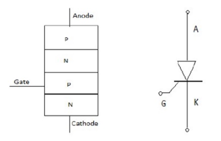
SCR is made up of silicon, it act as a rectifier; it has very low resistance in the forward direction and high resistance in the reverse direction. It is a unidirectional device.
1. Static V-I characteristics of a Thyristor
The circuit diagram for obtaining static V-I characteristics is as shown
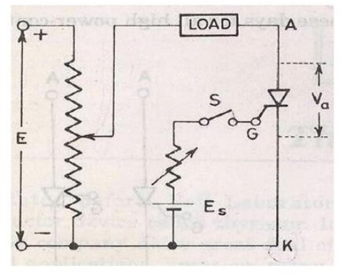
Anode and cathode are connected to main source voltage through the load. The gate and cathode are fed from source ES.
A typical SCR V-I characteristic is as shown below:
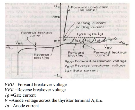
It can be inferred from the static V-I characteristic of SCR.
2. Modes of operation
SCR have 3 modes ofoperation:
1. Reverse blocking mode
2. Forward blocking mode ( off state)
3. Forward conduction mode (on state)
1. Reverse Blocking Mode
When cathode of the thyristor is made positive with respect to anode with switch open thyristor is reverse biased. Junctions J 1 and J 2 are reverse biased where junction J 2 is forward biased. The device behaves as if two diodes are connected in series with reverse voltage applied across them.
A small leakage current of the order of few mA only flows. As the thyristor is reverse biased and in blocking mode. It is called as acting in reverse blocking mode of operation.
Now if the reverse voltage is increased, at a critical breakdown level called reverse breakdown voltageVB,an avalanche occurs at J 1 and J 3 and the reverse current increases rapidly. As a large current associated with and hence more losses to the SCR. This results in Thyristor damage as junction temperature may exceed its maximum temperature rise.
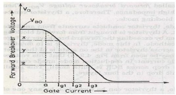
2. Forward Blocking Mode
When anode is positive with respect to cathode, with gate circuit open, thyristor is said tobe forward biased. Thus junction I1 and I 3 are forward biased and I 2 is reverse biased. As the forward voltage is increases junction I 2 will have an avalanche breakdown at a voltage called forward breakover voltageVB . When forward voltage is less then VB0 thyristor offers high impedance. Thus a thyristor acts as an open switch in forward blocking mode.
3. Forward Conduction Mode
Here thyristor conducts current from anode to cathode with a very small voltage dropacross it. So a thyristor can be brought from forward blocking mode to forwardconducting mode:
1. By exceeding the forward breakover voltage.
2. By applying a gate pulse between gate and cathode.
During forward conduction mode of operation thyristor is in on state and behave like aclose switch. Voltage drop is of the order of 1 to 2mV. This small voltage drop is due toohmic drop across the four layers of the device.
3. Turn ON methods
Different turn ON methods for SCR
1. Forward voltage triggering
2. Gate triggering
3. dv/dt triggering
4. Light triggering
5. Temperature triggering
1. Forward voltage triggering
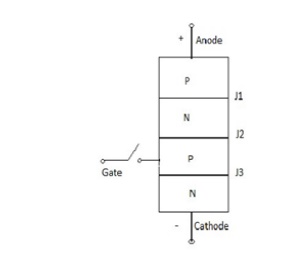
A forward voltage is applied between anode and cathode with gate circuit open. A forward voltage is applied between anode and cathode with gate circuit open. Junction J1 and J 3 is forward biased.
Juntion J 2 is reverse biased.
As the anode to cathode voltage is increased breakdown of the reverse biased junction J 2 occurs. This is known as avalanche breakdown and the voltage at which this phenomena occurs is called forward break over voltage.The conduction of current continues even if the anode cathode voltage reduces below VBO till Ia will not go below ℎ .Where ℎ is the holding current for the thyristor.
2. Gate triggering
This is the simplest, reliable and efficient method of firing the forward biased SCRs. FirstSCR is forward biased. Then a positive gate voltage is applied between gate and cathode. Inpractice the transition from OFF state to ON state by exceeding VBO is never employed as itmay destroy the device. The magnitude of ,so forward breakover voltage is taken as finalvoltage rating of the device during the design of SCR application.
First step is to choose a thyristor with forward breakover voltage (say 800V) higher than thenormal working voltage. The benefit is that the thyristor will be in blocking state with normal working voltage applied across the anode and cathode with gate open. When we require theturning ON of a SCR a positive gate voltage between gate and cathode is applied. The pointto be noted that cathode n- layer is heavily doped as compared to gate p-layer. So when gate supply is given between gate and cathode gate p-layer is flooded with electron from cathoden-layer. Now the thyristor is forward biased, so some of these electron reach junction J2 .As aresult width of 2 breaks down or conduction at J2 occur at a voltage less than VBO . As increases VBO reduces which decreases then turn ON time. Another important point isduration for which the gate current is applied should be more then turn ON time. This meansthat if the gate current is reduced to zero before the anode current reaches a minimum valueknown as holding current, SCR can‟t turn ONIn this process power loss is less and also low applied voltage is required for triggering.
3. dv/dt triggering
This is a turning ON method but it may lead to destruction of SCR and so it must be avoided.
When SCR is forward biased, junction J1 and J3 are forward biased and junction J2 isreversed biased so it behaves as if an insulator is place between two conducting plate. Here J1and J3 acts as a conducting plate and J2 acts as an insulator. J2 is known as junction capacitor. So if we increase the rate of change of forward voltage instead of increasing the magnitude ofvoltage. Junction J2 breaks and starts conducting. A high value of changing current maydamage the SCR. So SCR may be protected from high .
4. Temperature triggering
During forward biased, J2 is reverse biased so a leakage forward current always associated with SCR. Now as we know the leakage current is temperature dependant, so if we increase the temperature the leakage current will also increase and heat dissipitation of junction J2 occurs. When this heat reaches a sufficient value J2 will break and conduction starts.
Disadvantages
This type of triggering causes local hot spot and may cause thermal run away of the device. This triggering cannot be controlled easily.It is very costly as protection is costly.
5. Light triggering
First a new recess niche is made in the inner p-layer. When this recess is irradiated, then freecharge carriers (electron and hole) are generated. Now if the intensity is increased above acertain value then it leads to turn ON of SCR. Such SCR are known as Light activated SCR(LASCR).
Latching current
The latching current may be defined as the minimum value of anode current which at mustattain during turn ON process to maintain conduction even if gate signal is removed.
Holding current
It is the minimum value of anode current below which if it falls, the SCR will turn OFF.
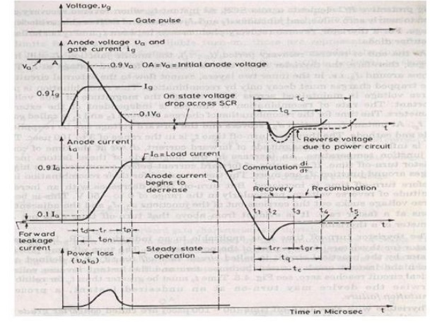
4. Switching characteristics of thyristors
The time variation of voltage across the thyristor and current through it during turn onand turn off process gives the dynamic or switching characteristic of SCR.
Switching characteristic during turn on Turn on time
It is the time during which it changes from forward blocking state to ON state. Total turnon time is divided into 3 intervals:
1. Delay time
2. Rise time
3. Spread time
Delay time
If Ig and Ia represent the final value of gate current and anode current. Then the delay timecan be explained as time during which the gate current attains 0.9 Ig to the instant anode current reaches 0.1Ig or the anode current rises from forward leakage current to 0.1 I .
1. Gate current 0.9 Ig to 0.1 I .
2. Anode voltage falls from V to 0.9 aa.
3. Anode current rises from forward leakage current to 0.1 I.
Rise time (t)
Time during which
1. Anode current rises from 0.1Ia to 0.9 Ia
2. Forward blocking voltage falls from 0.9 Vto 0.1V . is the initial forward blocking anode voltage.
Spread time (t )
1. Time taken by the anode current to rise from 0.9 Ia to I.
2. Time for the forward voltage to fall from 0.1 V to on state voltage drop of 1 to 1.5V. During turn on, SCR is considered to be a charge controlled device. A certain amount of charge is injected in the gate region to begin conduction. So higher the magnitude of gate current it requires less time to inject the charges. Thus turn on time is reduced by using large magnitude of gate current.
Switching Characteristics During Turn Off
Thyristor turn off means it changed from ON to OFF state. Once thyristor is ON there isno role of gate. As we know thyristor can be made turn OFF by reducing the anodecurrent below the latching current. Here we assume the latching current to be zeroampere. If a forward voltage is applied across the SCR at the moment it reaches zero thenSCR will not be able to block this forward voltage. Because the charges trapped in the 4-layer are still favourable for conduction and it may turn on the device. So to avoid such acase, SCR is reverse biased for some time even if the anode current has reached to zero.
So now the turn off time can be different as the instant anode current becomes zero to theinstant when SCR regains its forward blocking capability.
t (q)= t(rr) + t(qr)
Where,
is the turn off time, is the reverse recovery time, tqr is the gate recovery time At 1 anode current is zero. Now anode current builds up in reverse direction with same dv/dt slope. This is due to the presence of charge carriers in the four layers. The reverse recovery current removes the excess carriers from J1 and J3 between the instants J1 and J3 .At instant 3 the end junction J1 and J3 is recovered. But J2 still has trapped charges which decay due to recombination only so the reverse voltage has to be maintained for some more time. The time taken for the recombination of charges between J3 and J4 is called gate recovery time tq . Junction J2 recovered and now a forward voltage can be applied across SCR.
The turn off time is affected by:
1. Junction temperature
2. Magnitude of forward current
Turn off time decreases with the increase of magnitude of reverse applied voltage.
Related Topics