Chapter: Power Electronics : Power Semi Conductor Devices
Power MOSFET
POWER MOSFET
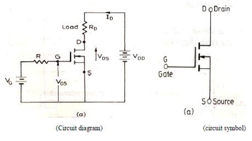
A power MOSFET has three terminal device. Arrow indicates the direction of current flow. MOSFET is a voltage controlled device. The operation of MOSFET depends on flow of majority carriers only.

1. Switching Characteristics:-
The switching characteristic is influenced by
1. Internal capacitance of the device.
2. Internal impedance of the gate drive circuit.
Total turn on time is divided into
1.Turn on delay time
2.Rise time
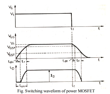
Turn on time is affected by impedance of gate drive source. During turn on delay time gate to source voltage attends its threshold value .
After tdn and during rise time gate to source voltage rise to VGsp , a voltage which is sufficient to drive the MOSFET to ON state.
The turn off process is initiated by removing the gate to source voltage. Turn off time is composed of turn off delay time to fall time.
Turn off delay time To turn off the MOSFET the input capacitance has to be discharged . During tdf the input capacitance discharge from V1to VGsp . During , fall time ,the input capacitance discharges from VGsp to VGST . During drain current falls from ID to zero. So when VGs ≤ , MOFSET turn off is complete.

Insulated Gate Bipolar Transistor (IGBT)
IGBT has high input impedance like MOFFSET and low on state power lose as in BJT.
2. IGBT Characteristics
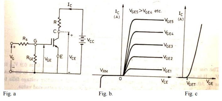
Here the controlling parameter is gate emitter voltage As IGBT is a voltage controlled device. When VGE is less than VGET that is gate emitter threshold voltage IGBT is in off state.

Fig. a (Circuit diagram for obtaining V-I characteristics) Fig. b (Static V-I characteristics)
Fig. c (Transfer characteristic)
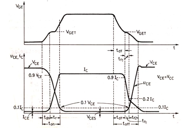
Switching characteristics: Figure below shows the turn ON and turn OFF characteristics of IGBT
Turn on

Turn on time :
Time between the instants forward blocking state to forward on -state .
Turn on time = Delay time + Rise time
Delay time = Time for collector emitter voltage fall from VCE to 0.9 VCEVCE =Initial collector emitter voltage
tdn =collector current to rise from initial leakage current to 0.1Ic
Ic= Final value of collector current
Rise time:
Collector emitter voltage to fall from 0.9 VCE to 0.1 VCE . 0.1Ic to Ic
After ton the device is on state the device carries a steady current of Ic and the collector emitter voltage falls to a small value called conduction drop VCES .
Turn off time :
1) Delay time tdf
2) Initial fall time tf1
3) Final fall time tf2
Toff = tdf + tf1 + tf2
tdf = Time during which the gate emitter voltage falls to the threshold value VGEF . Collector current falls from Ic to 0.9Ic at the end of the td collector emitter voltage begins to rise. Turn off time = Collector current falls from 90% to 20% of its initial value Ic OR The time during which collector emitter voltage rise from to 0.1 .
tf2=collector current falls from20% to 10% of Ic. During this collector emitter voltage rise 0.1VCE to final value of VCE .
Related Topics