Chapter: Electronic Circuits : Wave Shaping and Multivibrator Circuits
Positive and Negative Clamper
Clamper
The clamping network is one that will ―clamp a
signal to a different dc level. The network must have a capacitor, a diode, and
a resistive element, but it can also employ an independent dc supply to
introduce an additional shift. The magnitude of R and C must be chosen such
that the time constant τ= RC is large enough to ensure that the voltage across
the capacitor does not discharge significantly during the interval the diode is
non conducting.
Throughout the analysis we will assume that for
all practical purposes the capacitor will fully charge or discharge in five
time constants. The network of Fig. will clamp the input signal to the zero
level (for ideal diodes). The resistor R can be the load resistor or a parallel
combination of the load resistor and a resistor designed to provide the desired
level of R.
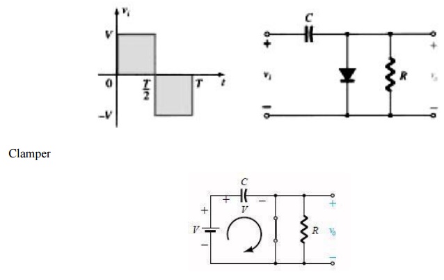
Diode ―on and the capacitor charging to V
volts.
During the interval 0 → T/2 the network will
appear, with the diode in the ―on state effectively ―shorting out the effect of
the resistor R. The resulting RC time constant is so small (R determined by the
inherent resistance of the network) that the capacitor will charge to V volts
very quickly. During this interval the output voltage is directly across the
short circuit and Vo =0 V. When the input switches to the -V state,
the network will appear With an open circuit equivalent for the diode
determined by the applied signal and stored voltage across the capacitor—both
―pressuring current through the diode from cathode to anode.
Now that R is back in the network the time
constant determined by the RC product is sufficiently large to establish a
discharge period much greater than the period T/2 → T, and it can be assumed on
an approximate basis that the capacitor holds onto all its charge and,
therefore, voltage (since V = Q/C) during this period. Since vo is in
parallel with the diode and resistor, it can also be drawn in the alternative
position shown in Fig. 2.94. Applying Kirchhoff‘s voltage law around the input
loop will result in -V – V – Vo = 0vand Vo =2V
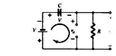
Determining Vo with the diode ―off.
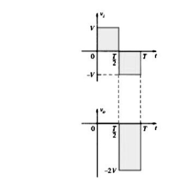
Sketching Vo for the network
The negative sign resulting from the fact that
the polarity of 2V is opposite to the polarity defined for Vo. The resulting
output waveform appears with the input signal. The output signal is clamped to
0 V for the interval 0 to T/2 but maintains the same total swing (2V) as the
input. For a clamping network:
The total swing of the output is equal to the
total swing of the input signal.
This fact is an excellent checking tool for the
result obtained. In general, the following steps may be helpful when analyzing
clamping networks:
1. Start the analysis of clamping systems by
considering that part of the input signal that will forward bias the diode. The
statement above may require skipping an interval of the input signal (as
demonstrated in an example to follow), but the analysis will not be extended by
an unnecessary measure of investigation.
During the period that the diode is in the ―on
state, assume that the capacitor will charge up instantaneously to a voltage
level determined by the network.
3. Assume that during the period when the diode is
in the ―off state the capacitor will hold on to its established voltage level.
4. Throughout the analysis maintain a continual
awareness of the location and reference polarity for to ensure that the proper
levels for are obtained.
5. Keep in mind the general rule that the total
swing of the total output must match the swing of the input signal .
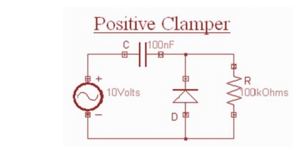
1. Positive Clamper
During the negative half cycle of the input
signal, the diode conducts and acts like a short circuit. The output voltage Vo
0 volts . The capacitor is charged to the peak value of input voltage Vm. and
it behaves like a battery.During the positive half of the input signal, the
diode does not conduct and acts as an open circuit. Hence the output voltage Vo=
Vm+ Vm This gives a positively clamped voltage
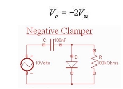
2. Negative Clamper
During the positive half cycle the diode
conducts and acts like a short circuit. The capacitor charges to peak value of
input voltage Vm. During this interval the output Vo
which is taken across the short circuit will be zero During the negative half
cycle, the diode is open. The output voltage can be found by applying KVL.
Related Topics