Chapter: Electronic Circuits : Wave Shaping and Multivibrator Circuits
Astable and Bistable Multivibrators
Multivibrators
Introduction
The type of circuit most often used to generate
square or rectangular waves is the multivibrator. A multivibrator, is basically
two amplifier circuits arranged with regenerative feedback. One of the
amplifiers is conducting while the other is cut off When an input signal to one
amplifier is large enough, the transistor can be driven into cutoff, and its
collector voltage will be almost V CC. However, when the transistor is driven
into saturation, its collector voltage will be about 0 volts.
A circuit that is designed to go quickly from
cutoff to saturation will produce a square or rectangular wave at its output.
This principle is used in multivibrators. Multivibrators are classified
according to the number of steady (stable) states of the circuit. A steady
state exists when circuit operation is essentially constant; that is, one
transistor remains in conduction and the other remains cut off until an
external signal is applied.
The three types of multivibrators :
ü ASTABLE
ü MONOSTABLE
ü BISTABLE.
The astable circuit has no stable state. With
no external signal applied, the transistors alternately switch from cutoff to
saturation at a frequency determined by the RC time constants of the coupling
circuits.
The monostable circuit has one stable state;
one transistor conducts while the other is cut off. A signal must be applied to
change this condition. After a period of time, determined by the internal RC
components, the circuit will return to its original condition where it remains
until the next signal arrives.
The bistable multivibrator has two stable
states. It remains in one of the stable states until a trigger is applied. It
then FLIPS to the other stable condition and remains there until another
trigger is applied. The multivibrator then changes back (FLOPS) to its first
stable state.
1. Astable Multivibrator
A multivibrator which generates square waves of
its own (i.e. without any external trigger pulse) is known as astable
multivibrator. It is also called free ramming multivibrator. It has no stable
state but only two quasi-stables (half-stable) makes oscillating continuously
between these states. Thus it is just an oscillator since it requires no
external pulse for its operation of course it does require D.C power.
In such circuit neither of the two transistors
reaches a stable state. It switches back and forth from one state to the other,
remaining in each state for a time determined by circuit constants. In other
words, at first one transistor conducts (i.e. ON state) and the other stays in
the OFF state for some time. After this period of time, the second transistor
is automatically turned ON and the first transistor turned OFF. Thus the
multivibrator will generate a square wave of its own. The width of the square
wave and it frequency will depend upon the circuit constants.
Here we like to describe.
ü Collector - coupled Astabe multivibrator
ü Emitter - coupled Astable multivibrator
Figure (a) shows the circuit of a collector
coupled astable multivibrator using two identical NPN transistors Q1
and Q2. It is possible to have RL1 = RL2 = RL
= R1 = R2 = R and C1 = C2 = C. In
that case , the circuit is known as symmetrical astable multivibrator. The
transistor Q1 is forward biased by the Vcc supply through
resistor R2. Similarly the transistor Q2 is
forward biased by the Vcc supply through resistor R1.
The output of transistor Q1 is coupled to the input of transistor Q2
through the capacitor C2. Similarly the output of transistor
Q2 is coupled to the input of transistor Q1 through the capacitor
C1.
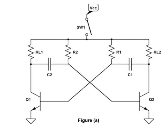
It consists of two common emitter amplifying
stages. Each stage provides a feedback through a capacitor at the input of the
other. Since the amplifying stage introduces a 180o phase shift and
another 180o phase shift is introduced by a capacitor, therefore the
feedback signal and the circuit works as an oscillator. In other words because
of capacitive coupling none of the transistor can remain permanently out-off or
saturated, instead of circuit has two quasi-stable states (ON and OFF) and it
makes periodic transition between these two states.
The output of an Astable multivibrator is
available at the collector terminal of the either transistors as shown in
figure (a). However, the two outputs are 180o out of phase with each
other. Therefore one of the outputs is said to be the complement of the other.
Let us suppose that
When Q1is ON, Q2 is OFF
and
When Q2 is ON, Q1 is OFF.
When the D.C power supply is switched ON by
closing S, one of the transistors will start conducting before the other (or
slightly faster than the other). It is so because characteristics of no two
similar transistors can be exactly alike suppose that Q1 starts
conducting before Q2 does. The feedback system is such that Q1
will be very rapidly driven ton saturation and Q2 to cut-off. The
circuit operation may be explained as follows.
Since Q1 is in saturation whole of VCC
drops across RL1. Hence VC1 = 0 and point A is at zero or
ground potential. Since Q2 is in cut-off i.e. it conducts no
current, there is no drop across R L2. Hence point B is at VCC.
Since A is at 0V C2 starts to charge through R2 towards VCC.
When voltage across C2 rises
sufficiently (i.e. more than 0.7V), it biases Q2 in the forward
direction so that it starts conducting and is soon driven to saturation.
VCC decreases and becomes almost
zero when Q2 gets saturated. The potential of point B decreases from
VCC to almost 0V. This potential decrease (negative swing) is
applied to the base of Q1 through C1. Consequently, Q1
is pulled out of saturation and is soon driven to cut-off.
Since, now point B is at 0V, C1
starts charging through R1 towards the target voltage VCC.
When voltage of C1 increases sufficiently. Q1
becomes forward-biased and starts conducting. In this way the whole cycle is
repeated.
It is observed that the circuit alternates
between a state in which Q1 is ON and Q2 is OFF and the
state in which Q1 is OFF and Q2 is ON. This time in each
state depends on RC values. Since each transistor is driven alternately into
saturation and cut-off. The voltage waveform at either collector (points A and
B in figure (b)) is essentially a square waveform with peak amplitude equal to VCC.
Calculation
of switching times and frequency of oscillations:
The frequency of oscillations can be calculated
by charging and discharging capacitances and its base resistance RB.
The voltage across the capacitor can be written
as
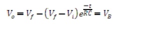
Vi= intial voltage = VB
=-VCC thus the transistors enters from ON to OFF state
Vf = final voltage = VB =
-VCC then the resistor enters from OFF to ON state
T1 is ON & T2 is
OFF the above equation can be written as
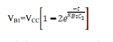
substitute
at t=T1, VB1=0 hence this equation becomes
T1=.69RB2C2
The total time period T=.694(RB1C1+RB2C2)
When RB!=RB2=R & C1=C2=C
T=1.39RC
Frequency of free running multivibrator is
given by
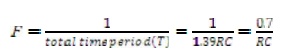
the frequency stability of the circuit is not
good as only the function of the product of RC but also depends on load
resistances, supply voltages and circuit parameters. In order to stabilize the
frequency, synchronizing signals are injected which terminate the unstable
periods earlier than would occur naturally.
2. Bistable multivibrator
The bistable multivibrator has two absolutely
stable states. It will remain in whichever state it happens to be until a
trigger pulse causes it to switch to the other state. For instance, suppose at
any particular instant, transistor Q1 is conducting and
transistor Q 2 is at cut-off. If left to itself, the bistable
multivibrator will stay in this position for ever. However, if an external
pulse is applied to the circuit in such a way that Q1 is cut-off and
Q2 is turned on, the circuit will stay in the new position. Another
trigger pulse is then required to switch the circuit back to its original
state.
In other words a multivibrator which has both
the state stable is called a bistable multivibrator. It is also called
flip-flop, trigger circuit or binary. The output pulse is obtained when, and
why a driving (triggering) pulse is applied to the input. A full cycle of
output is produced for every two triggering pulses of correct polarity and
amplitude.
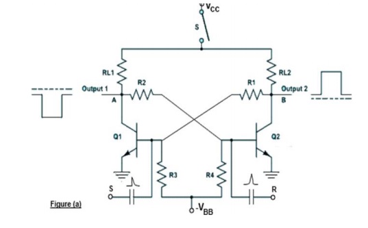
Figure (a) shows the circuit of a bistable
multivibrator using two NPN transistors. Here the output of a transistor Q2
is coupled put of a transistor Q1 through a resistor R2.
Similarly, the output of a transistor Q1 is coupled to the base of
transistor Q2 through a resistor R1. The
capacitors C 2 and C1 are known as speed up capacitors.
Their function is to increase the speed of the circuit in making abrupt
transition from one stable state to another stable state. The base resistors (R3
and R4) of both the transistors are connected to a common source (-VBB).
The output of a bistable multivibrator is available at the collector terminal
of the both the transistor Q1 and Q. However, the two outputs are
the complements of each other.
Let us suppose, if Q1 is conducting,
then the fact that point A is at nearly ON makes the base of Q2
negative (by the potential divider R2 - R4) and holds Q2
off.
Similarly with Q2 OFF, the potential
divider from VCC to -VBB (RL2, R1,
R3) is designed to keep base of Q1 at about 0.7V ensuring
that Q1 conducts. It is seen that Q1 holds Q2
OFF and Q2 hold Q1 ON. Suppose, now a positive pulse is
applied momentarily to R. It will cause Q2 to conduct. As collector
of Q2 falls to zero, it cuts Q1 OFF and consequently, the
BMV switches over to its other state.
Similarly, a positive trigger pulse applied to
S will switch the BMV back to its original state.
Uses:
ü In timing circuits as frequency divider
ü In counting circuits
ü In computer memory circuits
Bistable
Multivibrator Triggering
To change the stable state of the binary it is
necessary to apply an appropriate pulse in the circuit, which will try to bring
both the transistors to active region and the resulting regenerative feedback
will result on the change of state.
Triggering may be of two following types:
Asymmetrical triggering
Symmetrical triggering
(I) Asymmetrical triggering
In asymmetrical triggering, there are two
trigger inputs for the transistors Q1 and Q2. Each
trigger input is derived from a separate triggering source. To induce
transition among the stable states, let us say that initially the trigger is
applied to the bistable. For the next transition, now the identical trigger
must appear at the transistor Q2. Thus it can be said that the
asymmetrical triggering the trigger pulses derived from two separate source and
connected to the two transistors Q1 and Q2 individually,
sequentially change the state of the bistable.
Figure (b) shows the circuit diagram of an
asymmetrically triggered bistable multivibrator.
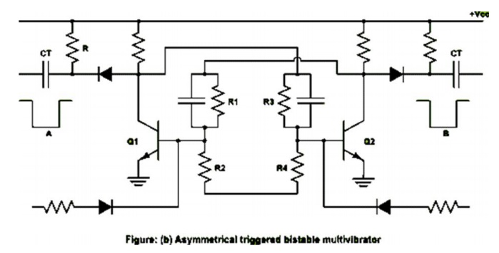
Initially Q1 is OFF and transistor Q2
is ON. The first pulse derived from the trigger source A, applied to the
terminal turn it OFF by bringing it from saturation region to active transistor
Q1 is ON and transistor Q2 is OFF. Any further pulse next
time then the trigger pulse is applied at the terminal B, the change of stable
state will result with transistor Q2 On and transistor Q1
OFF.
Asymmetrical triggering finds its application
in the generation of a gate waveform, the duration of which is controlled by
any two independent events occurring at different time instants. Thus
measurement of time interval is facilitated.
(II) symmetrical triggering
There are various symmetrical triggering
methods called symmetrical collector triggering, symmetrical base triggering
and symmetrical hybrid triggering. Here we would liked to explain only
symmetrical base triggering (positive pulse) only as given under symmetrical
Base Triggering.
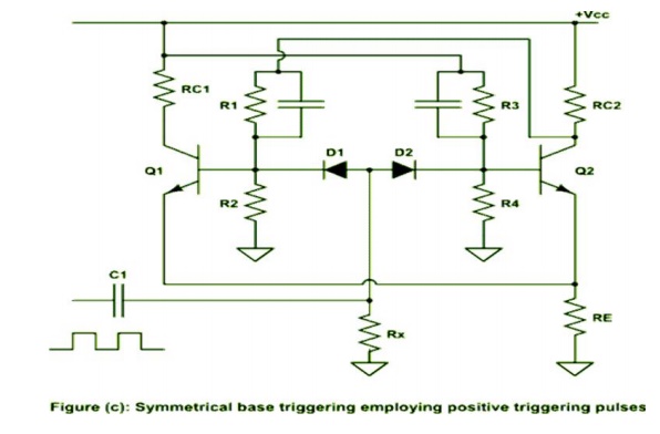
Figure (c) shows the circuit diagram of a
binary with symmetrical base triggering applying a positive trigger pulses.
Diodes D1 and D2 are
steering diodes. Here the positive pulses, try to turn ON and OFF transistor.
Thus when transistor Q1 is OFF and transistor Q2 is ON,
the respective base voltages and VB1N, OFF and V B2N, ON.
It will be seen that VB1N, OFF > VB1N, ON. Thus diode
D2 is more reverse-biased compared to diode D1.
When the positive differentiated pulse of
amplitude greater than (VB1N, OFF + Vɣ) appears, the diode D1
gets forward biased, and transistor Q1 enters the active region and
with subsequent regenerative feedback Q1 gets ON, and transistor Q2
becomes OFF. On the arrival of the next trigger pulse now the diode D2
will be forward biased and ultimately with regenerative feedback it will be in
the ON state.
Related Topics