Chapter: Digital Electronics : Combinational Circuits
Parity Generator and Checker
PARITY GENERATOR AND CHECKER:
§ A parity bit added to n-bit code to produce an
n + 1 bit code:
•
Add odd
parity bit to generate code words with even parity
•
Add even
parity bit to generate code words with odd parity
•
Use odd
parity circuit to check code words with even parity
•
Use even
parity circuit to check code words with odd parity
§ Example: n = 3. Generate even parity code words
of length four with odd parity generator:
§ Check even parity code words of length four
with odd parity checker: Operation: (X,Y,Z) = (0,0,1) gives (X,Y,Z,P) =
(0,0,1,1) and E = 0.
If Y
changes from 0 to 1 between generator and checker, then E = 1 indicates an
error
Often,
external noise will corrupt binary information (cause a bit to flip from one
logic state to the other) as it travels along a conductor from one device to
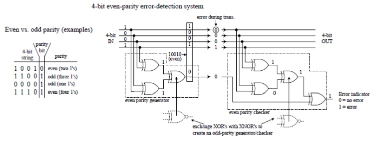
the next. For example, in the 4-bit system shown in Fig. 12.51, a BCD 4 (0100)
picks up noise and becomes 0101 (or 5) before reaching its destination.
Depending on the application, this type of error could lead to some serious
problems.
To avoid
problems caused by unwanted data corruption, a parity generator/ checker
system, like the one shown in Fig can be used.
The
basic idea is to add an extra bit, called a parity
bit, to the digital information being transmitted. If the parity bit makes
thesumof all transmitted bits (including the parity bit) odd, the transmitted
information is of odd parity.
If the
parity bit makes the sum even, the transmitted information is of even parity. Aparity
generator circuit creates the parity bit, while the parity checker on the
receiving end determines if the information sent is of the proper parity.
The type
of parity (odd or even) is agreed to beforehand, so the parity checker knows
what to look for. The parity bit can be placed next to the MSB or the LSB,
provided the device on the receiving end knows which bit is the parity bit and
which bits are the data. The arrangement shown in Fig is designed with an
even-parity error-detection system.

If you
want to avoid building parity generators and checkers from scratch, use a
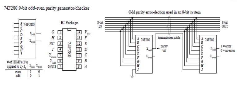
parity generator/checker IC like the 74F280 9-bit odd-even parity
generator/checker shown below. To make a complete error-detection system, two
74F280s are used—one acts as the parity generator; the other acts as the parity
checker. The generator’s inputs A
through H are connected to the eight
data lines of the transmitting portion of the circuit. The ninth input (I) is grounded when the device is used
as a generator. If you want to create an odd-parity generator, you tap the Σodd
output; for even parity, you tap Σeven. The 74F280 checker taps the main line
at the receiving end and also accepts the parity bit line at input I. The figure below shows an odd-parity
error-detection system used with an 8-bit system. If an error occurs, a high
(1) is generated at the Σodd output.

Related Topics