Chapter: Optical Communication and Networking : Sources and Detectors
Optical Detectors
Optical Detectors
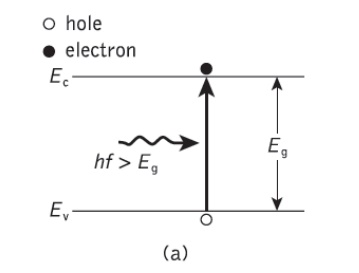
The basic detection process in an intrinsic absorber is illustrated in Figure 3.11 which shows a p–n photodiode. This device is reverse biased and the electric field developed across the p–n junction sweeps mobile carriers (holes and electrons) to their respective majority sides (p- and n-type material). A depletion region or layer is therefore created on either side of the junction. This barrier has the effect of stopping the majority carriers crossing the junction in the opposite direction to the field.
However, the field accelerates minority carriers from both sides to the opposite side of the junction, forming the reverse leakage current of the diode. Thus intrinsic conditions are created in the depletion region.

1. PIN Photo detectors
In order to allow operation at longer wavelengths where the light penetrates more deeply into the semiconductor material, a wider depletion region is necessary. To achieve this then-type material is doped so lightly that it can be considered intrinsic, and to make a low resistance contact a highly dopedn-type (n+) layer is added. This creates a p–i–n (or PIN) structure, as may be seen in Figure 3.12 where all the absorption takes place in the depletion region.
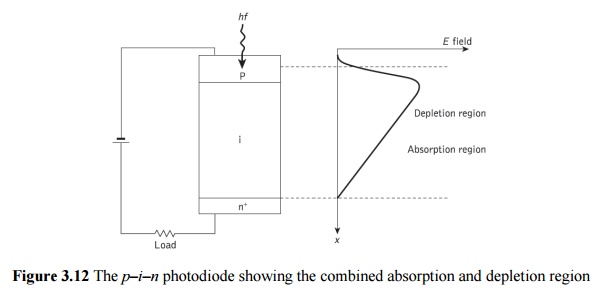
Figure 3.13 shows the structures of two types of silicon p–i–n photodiode for operation in the shorter wavelength band below 1.09 μm. The front-illuminated photodiode, when operating in the 0.8 to 0.9 μm band (Figure 3.13(a)), requires a depletion region of between 20 and 50 μm in order to attain high quantum efficiency (typically 85%) together with fast response (less than 1 ns) and low dark current (1 nA). Dark current arises from surface leakage currents as well as generation– recombination currents in the depletion region in the absence of illumination.
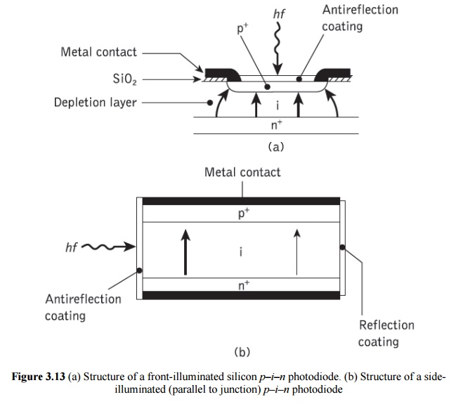
The side-illuminated structure (Figure 3.13(b)), where light is injected parallel to the junction plane, exhibits a large absorption width (_500 μm) and hence is particularly sensitive at wavelengths close to the bandgap limit (1.09 μm) where the absorption coefficient is relatively small. Germanium p–i–n photodiodes which span the entire wavelength range of interest are also commerciallyavailable, but as mentioned previously the relatively high dark currents are a problem (typically 100 nA at 20 °C increasing to 1 μA at 40 °C).
The favored material is the lattice-matched In0.53Ga0.47As/InP system which can detect at wavelengths up to 1.67 μm. A typical planar device structure is shown in Figure 3.14(a) which requires epitaxial growth of several layers on an n-type InP substrate. The incident light is absorbed in the low-doped n-type InGaAs layer generating carriers, as illustrated in the energy band diagram Figure 3.14(b). The discontinuity due to the homojunction between the n+-InP substrate and the n-InGaAs absorption region may be noted. This can be reduced by the incorporation of an n-type InP buffer layer.
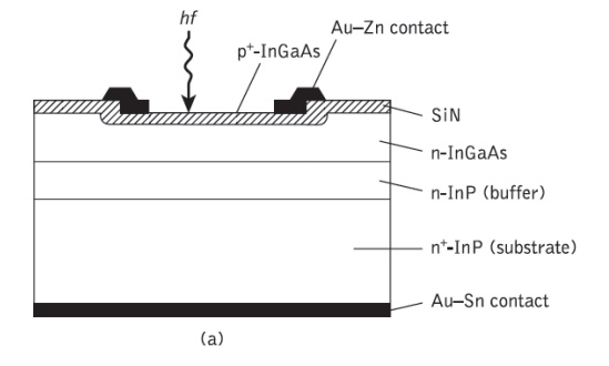
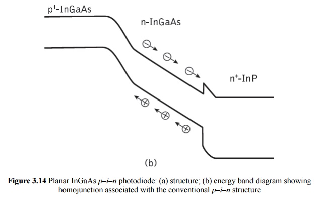
The top entry* device shown in Figure 3.14(a) is the simplest structure, with the light being introduced through the upper p+-layer. However, a drawback with this structure is a quantum efficiency penalty which results from optical absorption in the undepleted p+- region. In addition, there is a limit to how small such a device can be fabricated as both light access and metallic contact are required on the top. To enable smaller devices with lower capacitances to be made, a substrate entry technique is employed. In this case light enters through a transparent InP substrate and the device area can be fabricated as small as may be practical for bonding.
2. Avalanche photodiodes
The second major type of optical communications detector is the avalanche photodiode (APD). This has a more sophisticated structure than the p–i–nphotodiode in order to create an extremely high electric field region (approximately 3 × 10⁵ V cm−1), as may be seen in Figure 3.15(a). Therefore, as well as the depletion region where most of the photons are absorbed and the primary carrier pairs generated, there is a high-field region in which holes and electrons can acquire sufficient energy to excite new electron–hole pairs.
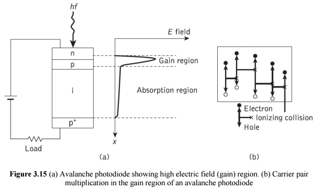
This process is known as impact ionization and is the phenomenon that leads to avalanche breakdown in ordinary reverse-biased diodes. It often requires high reverse bias voltages (50 to 400 V) in order that the new carriers created by impact ionization can themselves produce additional carriers by the same mechanism as shown in Figure 3.15(b). More recently, however, it should be noted that devices which will operate at much lower bias voltages (15 to 25 V) have become available.
Carrier multiplication factors as great as 104 may be obtained using defect-free materials to ensure uniformity of carrier multiplication over the entire photosensitive area. However, other factors affect the achievement of high gain within the device. Microplasmas, which are small areas with lower breakdown voltages than the remainder of the junction, must be reduced through the selection of defect-free materials together with careful device processing and fabrication.
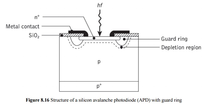
In addition, excessive leakage at the junction edges can be eliminated by the use of a guard ring structure as shown in Figure 3.16. At present silicon, germanium and InGaAs APDs are generally available.
Operation of these devices at high speed requires full depletion in the absorption region. When carriers are generated in undepleted material, they are collected somewhat slowly by the diffusion process. This has the effect of producing a long ‘diffusion tail’ on a short optical pulse. When the APD is fully depleted by employing electric fields in excess of 104 Vm−1, all the carriers drift at saturation-limited velocities. In this case the response time for the device is limited by three factors. These are:
(a)the transit time of the carriers across the absorption region (i.e. the depletion width);
(b) the time taken by the carriers to perform the avalanche multiplication process; and
(c) theRC time constant incurred by the junction capacitance of the diode and its load.
At low gain the transit time and RC effects dominate giving a definitive response time and hence constant bandwidth for the device. However, at high gain the avalanche build up time dominates and therefore the device bandwidth decreases proportionately with increasing gain. Such APD operation is distinguished by a constant gain–bandwidth product. Often an asymmetric pulse shape is obtained from the APD which results from a relatively fast rise time as the electrons are collected and a fall time dictated by the transit time of the holes traveling at a slower speed. Hence, although the use of suitable materials and structures may give rise times between 150 and 200 ps, fall times of 1 ns or more are quite common and limit the overall response of the device.
Related Topics