Chapter: Optical Communication and Networking : Sources and Detectors
Important Short Questions and Answers: Sources and Detectors of Optical
SOURCES AND DETECTORS
1.
What are
the advantages of optical communication?
1. Low
transmission loss.
2 Small
size and weight.
3. No
electromagnetic interference.
4. Electrical
isolation.
2.
Define
direct band gap materials and indirect band gap materials.
In direct band gap materials direct transition is possible from valence band to
conduction
band.e.g.GaAs,InP,InGaAs In indirect band gap materials direct transition is
not possible from valence band to conduction.e.g.silicon,germanium.
3.
What are
the advantages of LED?
1. LEDs are
less complex circuits than Laser diodes.
2. Fabrication
is easier.
3. They have
long life.
4.
What are
the two types of confinement used in LEDs?
1. Optical
confinement.
2. Carrier
confinement.
5.
What are
the two types of LED configurations?
1. Homo
junction
2. Single
and double hetero junction.
6.
What are
the three requirements of Laser action?
1. Absorption
2. Spontaneous
emission
3. stimulated
emission.
7.
What are
the three types of Laser diode structures?
1. Gain
indexed guide
2. Positive
indexed guide
3.Negative
indexed guide
8.
What are
the fundamental structures of Index guided lasers?
1. buried
hetero structure.
2. Selectively
diffused construction
3. Varying
thickness structure
4. Bent
layer configuration.
9.
What are
the three basic methods of current confinement?
1. Preferential
dopant diffusion.
2. Proton
implantation
3. Inner
strip confinement
4. Re growth
of back biased PN junction.
10.
Define
modulation.
The
process of imposing information on a light stream is called modulation. This
can be achieved by varying the laser drive current.
11. Define external quantum efficiency.
The
external quantum efficiency is defined as the number of photons emitted per
radiative electron-hole pair recombination above threshold.
12. Define threshold current.
The
threshold current is conventionally defined by extrapolation of the lasing
region of the power-versus-current curve. At high power outputs, the slope of
the curve decreases because of junction heating.
13. Define longitudinal modes.
Longitudinal
modes are associated with the length of the cavity and determine the typical
spectrum of the emitted radiation.
14. Define lateral modes.
These modes
lie in the plane o f t he p n junction. They depend on the side wall
preparation and the width of the cavity. It determines the shape of the lateral
profile of the laser beam.
15. Define transverse modes.
Transverse
modes are associated with the electromagnetic field and beam profile in the
direction perpendicular to the plane of the pn junction. They determine the
laser characteristics as the radiation pattern and the threshold current
density.
16. Define population inversion.
Stimulated
emission will exceed absorption only if the population of the excited states is
greater than that of the ground state. This condition is called as population
inversion
17. Define internal quantum efficiency.
The
internal quantum efficiency is the fraction of the electron-hole pairs that
recombine radiatively. If the radiative recombination rate is R and the
non-radiative recombination rate is Rnr, then the internal quantum efficiency
is the ratio of the ratio of the radiative recombination rate to the total
recombination rate.
18. Differentiate LEDs and Laserdiodes.
LED
1. The output obtained is incoherent.
2. Less expensive and less complex
3. Long lifetime.
Laser diode
1. The output obtained is coherent.
2. More expensive and more complex.
3. Less lifetime.
Where
p-- concentration of holes.
n concentration of electrons.
Ni intrinsic concentration.
20.
What is
an intrinsic and extrinsic semiconductor material?
Intrinsic
semiconductors have no impurities.
Extrinsic
semiconductors contain impurities like boron and phosphorus.
21.
Define
responsivity
The performance o f an avalanche photodiode is characterized by its responsivity
RAPD= ηqM = Ro M hv
where
Ro is the
unity gain responsivity.
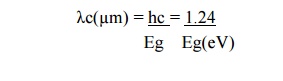
22. Define long wavelength cut off related to
photodiode.
The upper
wavelength cutoff (λc) is determined by the band gap energy Eg of the material.
If Eg is expressed in units of electron volts(eV),then λc is given in units of
micrometers (µm) by
23.
Give some
types of photodetectors.
•
Photomultipliers
•
Pyroelectric detectors
•
Semiconductor- based detectors
•
Phototransistors
•
Photodiodes
24.
What are
the advantages of photodiodes?
a. Small
size
b. Suitable
material c. High sensitivity
d. Fast
response time
25.
What are the
types of photodiodes?
•
PIN
photodetector
•
Avalanche photodiode(APD)
26.
Define
photocurrent.
The high
electric field present in the depletion region causes the carriers to separate
and be collected across the reverse-biased junction. This gives to a current
flow in the external circuit, with one electron flowing for every carrier pair
generated. This current flow is known as photocurrent.
27. Define quantum efficiency.
It is
defined as the number of the electron – hole pairs generated per incident photon
of energy hv and is given by
n=No.of
electron-hole pairs generated / No. of incident photons
28. Define impact ionization.
In order
for carrier multiplication to take place, the photo generated carriers must
traverse a region where a very high electric field is present. In this high
field region, a photo generated electron or hole can gain energy so that it
ionizes bound electrons in the valence band upon colliding with them. This
carrier multiplication mechanism is known as impact ionization.
29. Define avalanche effect.
The newly
created carriers are accelerated by the high electric field, thus gaining
enough energy to cause further impact ionization. This phenomenon is called
avalanche effect.
30. What is p+ ∏ p n+ reach- through structure?
The reach
–through avalanche photodiode (RAPD) is composed of a high resistivity p-type
material deposited as an epitaxial layer on a p+ substrate. A p- type diffusion
is then made in the high resistivity material, followed by the construction of
an n+ layer. The configuration is called p+ ∏ p n+ reach- through structure.
GLOSSARY
1. Direct band gap materials and indirect band
gap materials.
In direct
band gap materials direct transition is possible from valence band to
conduction band.e.g.GaAs,InP,InGaAs In indirect band gap materials direct
transition is not possible from valence band to
conduction.e.g.silicon,germanium.
2.
Advantages
of LED.
1. LEDs are
less complex circuits than Laser diodes.
2. Fabrication
is easier.
3. They have
long life.
3.
Two types
of confinement used in LEDs.
1. Optical
confinement.
2. Carrier
confinement.
4.
Modulation.
The
process of imposing information on a light stream is called modulation. This
can be achieved by varying the laser drive current.
5. External quantum efficiency.
The
external quantum efficiency is defined as the number of photons emitted per
radiative electron-hole pair recombination above threshold.
6. Threshold current.
The
threshold current is conventionally defined by extrapolation of the lasing
region of the power-versus-current curve. At high power outputs, the slope of
the curve decreases because of junction heating.
7. Longitudinal modes.
Longitudinal
modes are associated with the length of the cavity and determine the typical
spectrum of the emitted radiation.
8. Lateral modes.
These
modes lie in the plane of the p n junction. They depend on the side wall
preparation and the width of the cavity. It determines the shape of the lateral
profile of the laser beam.
9. Transverse modes.
Transverse
modes are associated with the electromagnetic field and beam profile in the
direction perpendicular to the plane of the pn junction. They determine the
laser characteristics as the radiation pattern and the threshold current
density.
10. Population inversion.
Stimulated
emission will exceed absorption only if the population of the excited states is
greater than that of the ground state. This condition is called as population
inversion
11. Internal quantum efficiency.
The
internal quantum efficiency is the fraction of the electron-hole pairs that
recombine radiatively. If the radiative recombination rate is R and the
non-radiative recombination rate is Rnr, then the internal quantum efficiency
is the ratio of the ratio of the radiative recombination rate to the total
recombination rate.
12. Intrinsic
and extrinsic semiconductor material.
Intrinsic
semiconductors have no impurities.
Extrinsic
semiconductors contain impurities like boron and phosphorus.
13. Responsivity
The performance o f an avalanche photodiode is characterized by its responsivity
RAPD= ηqM = Ro M hv
where
Ro is the
unity gain responsivity.
14. Long wavelength cut off related to photodiode.
The upper
wavelength cutoff (λc) is determined by the band gap energy Eg of the material.
If Eg is expressed in units of electron volts(eV),then λc is given in units of
micrometers (µm) by
15. Photocurrent.
The high
electric field present in the depletion region causes the carriers to separate
and be collected across the reverse-biased junction. This gives to a current
flow in the external circuit, with one electron flowing for every carrier pair
generated. This current flow is known as photocurrent.
16. Quantum efficiency.
It is
defined as the number of the electron – hole pairs generated per incident
photon of energy hv and is given by
n=No.of
electron-hole pairs generated /No. of incident photons
17. Impact ionization.
In order
for carrier multiplication to take place, the photo generated carriers must
traverse a region where a very high electric field is present. In this high
field region, a photo generated electron or hole can gain energy so that it
ionizes bound electrons in the valence band upon colliding with them. This
carrier multiplication mechanism is known as impact ionization.
18. Avalanche effect.
The newly
created carriers are accelerated by the high electric field, thus gaining
enough energy to cause further impact ionization. This phenomenon is called
avalanche effect.
Related Topics