Chapter: Optical Communication and Networking : Sources and Detectors
LED Structures
LED STRUCTURES
1. Surface emitter LEDs
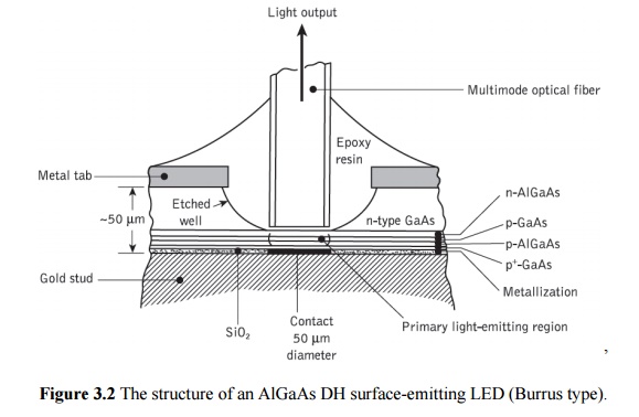
A method for obtaining high radiance is to restrict the emission to a small active region within the device. The technique pioneered by Burrus and Dawson with homostructure devices was to use an etched well in a GaAs substrate in order to prevent heavy absorption of the emitted radiation, and physically to accommodate the fiber. These structures have a low thermal impedance in the active region allowing high current densities and giving high-radiance emission into the optical fiber. Furthermore, considerable advantage may be obtained by employing DH structures giving increased efficiency from electrical and optical confinement as well as less absorption of the emitted radiation.
This type of surface emitter LED (SLED) has been widely employed within optical fiber communications. The structure of a high-radiance etched well DH surface emitter* for the 0.8 to 0.9μm wavelength band is shown in Figure 3.2. The internal absorption in this device is very low due to the larger bandgap-confining layers, and the reflection coefficient at the back crystal face is high giving good forward radiance. The emission from the active layer is essentially isotropic, although the external emission distribution may be considered Lambertian with a beam width of 120° due to refraction from a high to a low refractive index at the GaAs–fiber interface. The power coupled Pc into a multimode step index fiber may be estimated from the relationship:

where r is the Fresnel reflection coefficient at the fiber surface, A is the smaller of the fiber core cross-section or the emission area of the source andRD is the radiance of the source.
However, the power coupled into the fiber is also dependent on many other factors including the distance and alignment between the emission area and the fiber, the SLED emission pattern and the medium between the emitting area and the fiber. For instance, the addition of epoxy resin in the etched well tends to reduce the refractive index mismatch and increase the external power efficiency of the device. Hence, DH surface emitters often give more coupled optical power than predicted by Eq. (3.1).
However, for graded index fiber optimum direct coupling requires that the source diameter be about one-half the fiber core diameter. In both cases lens coupling may give increased levels of optical power coupled into the fiber but at the cost of additional complexity. Other factors which complicate the LED fiber coupling are the transmission characteristics of the leaky modes or large angle skew rays. Much of the optical power from an incoherent source is initially coupled into these large-angle rays, which fall within the acceptance angle of the fiber but have much higher energy than meridional rays. Energy from these rays goes into the cladding and may be lost.
Hence much of the light coupled into a multimode fiber from an LED is lost within a few hundred meters. It must therefore be noted that the effective optical power coupled into a short length of fiber significantly exceeds that coupled into a longer length.
The planar structure of the Burrus-type LED and other nonetched well SLEDs allows significant lateral current spreading, particularly for contact diameters less than 25 μm. This current spreading results in a reduced current density as well as an effective emission area substantially greater than the contact area.
2. Edge emitter LEDs
Another basic high-radiance structure currently used in optical communications is the stripe geometry DH edge emitter LED (ELED). This device has a similar geometry to a conventional contact stripe injection laser, as shown in Figure 3.3.
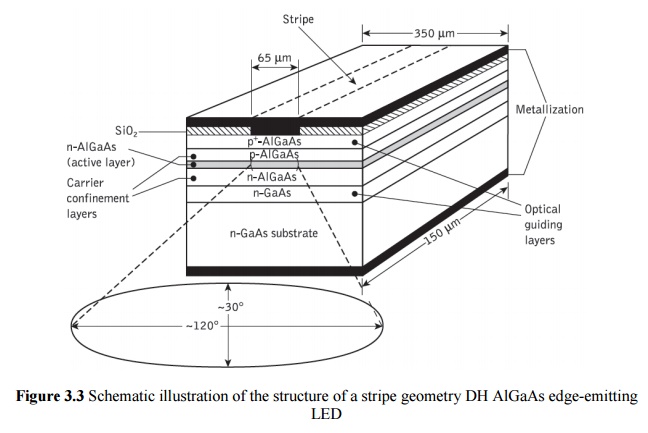
It takes advantage of transparent guiding layers with a very thin active layer (50 to 100 μm) in order that the light produced in the active layer spreads into the transparent guiding layers, reducing self-absorption in the active layer. The consequent waveguiding narrows the beam divergence to a half-power width of around 30° in the plane perpendicular to the junction. However, the lack of waveguiding in the plane of the junction gives a Lambertian output with a half-power width of around 120°, as illustrated in Figure3.3. Most of the propagating light is emitted at one end face only due to a reflector on the other end face and an antireflection coating on the emitting end face. The effective radiance at the emitting end face can be very high giving an increased coupling efficiency into small-NA fiber compared with the surface emitter. However, surface emitters generally radiate more powerinto air (2.5 to 3 times) than edge emitters since the emitted light is less affected by reabsorption and interfacial recombination. Comparisons have shown that edge emitters couple more optical power into low NA (less than 0.3) than surface emitters, whereas the opposite is true for large NA (greater than 0.3).
The enhanced waveguiding of the edge emitter enables it in theory to couple 7.5 times more power into low-NA fiber than a comparable surface emitter. However, in practice the increased coupling efficiency has been found to be slightly less than this (3.5 to 6 times). Similar coupling efficiencies may be achieved into low-NA fiber with surface emitters by the use of a lens. Furthermore, it has been found that lens coupling with edge emitters may increase the coupling efficiencies by comparable factors (around five times).
The stripe geometry of the edge emitter allows very high carrier injection densities for given drive currents. Thus it is possible to couple approaching a milliwatt of optical power into low-NA (0.14) multimode step index fiber with edge-emitting LEDs operating at high drive currents (500 mA).
Edge emitters have also been found to have a substantially better modulation bandwidth of the order of hundreds of megahertz than comparable surface-emitting structures with the same drive level. In general it is possible to construct edge-emitting LEDs with a narrower linewidth than surface emitters, but there are manufacturing problems with the more complicated structure (including difficult heat-sinking geometry) which moderate the benefits of these devices.
Related Topics