Chapter: Optical Communication and Networking : Sources and Detectors
Injection Laser Structures
Injection Laser Structures
1. Gain-guided lasers
Fabrication of multimode injection lasers with a single or small number of lateral modes is achieved by the use of stripe geometry. These devices are often called gain-guided lasers. The constriction of the current flow to the stripe is realized in the structure either by implanting the regions outside the stripe with protons (protonisolated stripe) to make them highly resistive, or by oxide or p–n junction isolation. The structure for an aluminum gallium arsenide oxide isolated stripe DH laserwas shown in Figure 3.6. It has an active region of gallium arsenide bounded on both sides by aluminum gallium arsenide regions. This technique has been widely applied, especially for multimode laser structures used in the shorter wavelength region. The current is confined by etching a narrow stripe in a silicon dioxide film.
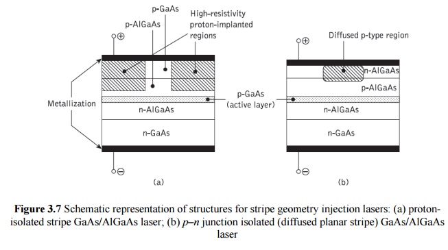
Two other basic techniques for the fabrication of gain-guided laser structures are illustrated in Figure3.7(a) and (b) which show the proton-isolated stripe and the p–n junction isolated stripe structures respectively. In Figure 3.7(a) the resistive region formed by the proton bombardment gives better current confinement than the simple oxide stripe and has superior thermal properties due to the absence of the silicon dioxide layer; p–n junction isolation involves a selective diffusion through the n-type surface region in order to reach the p-type layers, as illustrated in Figure 1(b). None of thesestructures confines all the radiation and current to the stripe region and spreading occurs on both sides of the stripe.
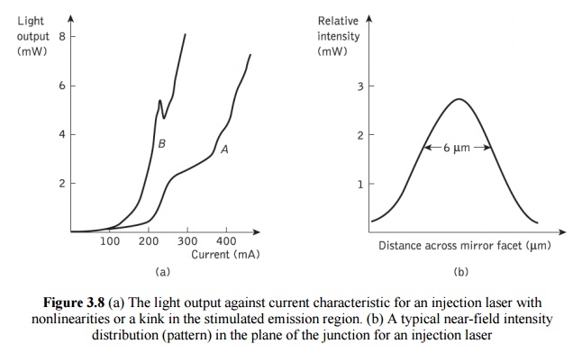
With stripe widths of 10 μm or less, such planar stripe lasers provide highly efficient coupling into multimode fibers, but significantly lower coupling efficiency is achieved into small-core-diameter single-mode fibers. However, with certain practical laser diodes the characteristic is not linear in the simulated emission region, but exhibits kinks. This phenomenon is particularly prevalent with gain-guided injection laser devices. The kinks may be classified into two broad categories.
The first type of kink results from changes in the dominant lateral mode of the laser as the current is changed. The output characteristic for laser A in Figure 3.8(a) illustrates this type of kink where lasing from the device changes from the fundamental lateral mode to a higher order lateral mode (second order) in a current region corresponding to a change in slope. The second type of kink involves a ‘spike’, as observed for laser B of Figure 3.8(a). These spikes have been shown to be associated with filamentary behavior within the active region of the device. The filaments result from defects within the crystal structure. Both these mechanisms affect the near- and far-field intensity distributions (patterns) obtained from the laser. A typical near-field intensity distribution corresponding to a single optical output power level in the plane of the junction is shown in Figure 3.8(b).
As this distribution is in the lateral direction, it is determined by the nature of the lateral waveguide. The single intensity maximum shown indicates that the fundamental lateral mode is dominant. To maintain such a near-field pattern the stripe geometry of the device is important. In general, relatively narrow stripe devices (< 10 μm) formed by a planar process allow the fundamental lateral mode to dominate.
This is especially the case at low power levels where near-field patterns similar to Figure 3.8(b) may be obtained. Although gain-guided lasers are commercially available for operation in both the shorter wavelength range (using GaAs active regions) and the longer wavelength range (using InGaAsP active regions) they exhibit several undesirable characteristics.
Apart from the nonlinearities in the light output versus current characteristics discussed above, gain-guided injection lasers have relatively high threshold currents (100 to 150 mA) as well as low differential quantum efficiency. These effects are primarily caused by the small carrier-induced refractive index reduction within the devices which results in the movement of the optical mode along the junction plane. The problems can be greatly reduced by introducing some real refractive index variation into the lateral structure of the laser such that the optical mode along the junction plane is essentially determined by the device structure.
2. Index-guided lasers
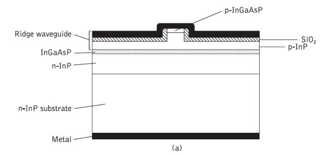
The drawbacks associated with the gain-guided laser structures were largely overcome through the development of index-guided injection lasers. In some such structures with weak index guiding, the active region waveguide thickness is varied by growing it over a channel or ridge in the substrate. A ridge is produced above the active region and the surrounding areas are etched close to it (i.e. within 0.2 to 0.3 μm). Insulating coatings on these surrounding areas confine the current flow through the ridge and active stripe while the edges of the ridge reflect light, guiding it within the active layer, and thus forming a waveguide. Hence in the ridge waveguide laser shown in Figure 3.9 (a), the ridge not only provides the location for the weak index guiding but also acts as the narrow current confining stripe. These devices have been fabricated to operate at various wavelengths with a single lateral mode, and room temperature CW threshold currents as low as 18 mA with output powers of 25 mW have been reported.
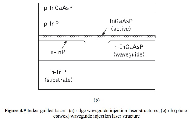
More typically, the threshold currents for such weakly index-guided structures are in the range 40 to 60 mA, which compares a light output versus current characteristic for a ridge waveguide laser with that of an oxide stripe gain-guided device. Alternatively, the application of a uniformly thick, planar active waveguide can be achieved through lateral variations in the confinement layer thickness or the refractive index. However, room temperature CW threshold currents are between 70 and 90 mA with output powers of around 20 mW for InGaAsP devices operating at a wavelength of 1.3 μm.
3. Quantum-well lasers
DH lasers have also been fabricated with very thin active layer thicknesses of around 10 nm instead of the typical range for conventional DH structures of 0.1 to 0.3 μm. The carrier motion normal to the active layer in these devices is restricted, resulting in a quantization of the kinetic energy into discrete energy levels for the carriers moving in that direction. This effect is similar to the well-known quantum mechanical problem of a one dimensional potential well and therefore these devices are known as quantumwell lasers. In this structure the thin active layer causes drastic changes to the electronic and optical properties in comparison with a conventional DH laser.
These changes are due to the quantized nature of the discrete energy levels with a step-like density of states which differs from the continuum normally obtained. Hence, quantum-well lasers exhibit an inherent advantage over conventional DH devices in that they allow high gain at low carrier density, thus providing the possibility of significantly lower threshold currents. Both single-quantum-well (SQW), corresponding to a single active region, and multiquantum-well (MQW), corresponding to multiple active regions, lasers are utilized. In the latter structure, the layers separating the active regions are called barrier layers. Energy band diagrams for the active regions of these structures are displayed in Figure 3.10. It may be observed in Figure 3.10(c) that when the bandgap energy of the barrier layer differs from the cladding layer in an MQW device, it is usually referred to as a modified multiquantum-well laser.
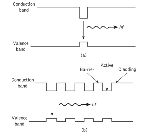
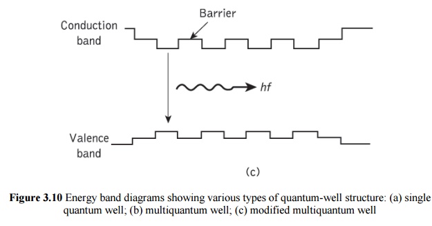
Better confinement of the optical mode is obtained in MQW lasers in comparison with SQW lasers, resulting in a lower threshold current density for these devices. A substantial amount of experimental work has been carried out on MQW lasers using the AlGaAs/GaAs material system. It has demonstrated the superior characteristics of MQW devices over conventional DH lasers in relation to lower threshold currents, narrower line widths, higher modulation speeds, lower frequency chirp and less temperature dependence.
Related Topics